
Radiative cooling substrate and manufacturing method of the same

a technology of radiative cooling and cooling substrate, which is applied in the direction of electrophoretic coating, coating, light and heating apparatus, etc., can solve the problems of affecting the general use of the structure, unsuitable daytime applications, etc., and achieve the commercial value of the particular waste, less harm to the environment, and dissipate thermal energy

Active Publication Date: 2021-08-03
NATIONAL TSING HUA UNIVERSITY
View PDF3 Cites 2 Cited by
  • Summary
  • Abstract
  • Description
  • Claims
  • Application Information

AI Technical Summary

Benefits of technology

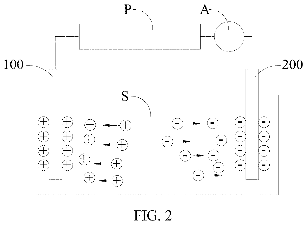
[0006]For the purpose of solving the foregoing problems, the present invention provides a radiative cooling substrate and a manufacturing method of the radiative cooling substrate. The main technical features of the present invention include depositing a chitosan layer on a metallic substrate in an electrophoretic process. In this way, the radiative cooling substrate does not absorb waves of solar radiation but has a high emissivity in the atmospheric window.
[0021](5) In comparison with the coating method in which a strong base solution is needed, the manufacturing method of the radiative cooling substrate of the present invention makes use of an water-based electrophoretic deposition process may not only provide a firmer deposition layer but also cause less harm to the environment, simplify the manufacturing process and reduce the production cost. In addition, the electrophoretic deposition process has big deposition areas, rarely produces creases or develops thermal contact resistance, and is not restricted by the shape of the substrate.

Problems solved by technology

However, these kinds of layers tend to absorb solar radiation of other wavebands and are hence unsuitable for daytime applications.
Further, for the foregoing structures combined with one-dimensional photonic crystals or metamaterials, there are some restrictions such as a complicate manufacturing process, including a requirement of coating an additional silver or aluminum layer with a thickness of several nanometers as a reflecting layer, which affects the general use of the structure.

Method used


Image

  • Radiative cooling substrate and manufacturing method of the same
  • Radiative cooling substrate and manufacturing method of the same
  • Radiative cooling substrate and manufacturing method of the same

Examples


Embodiment Construction

[0038]The advantages, features and technical methods of this invention will be described in detail in order to be understood easier. Moreover, the present invention may be realized in different form and should not be limited to the embodiments described here. On the contrary, the provided embodiments make the disclosure clear and define the scope of this invention entirely and completely. Further, the present invention is only defined according to the attached claims.

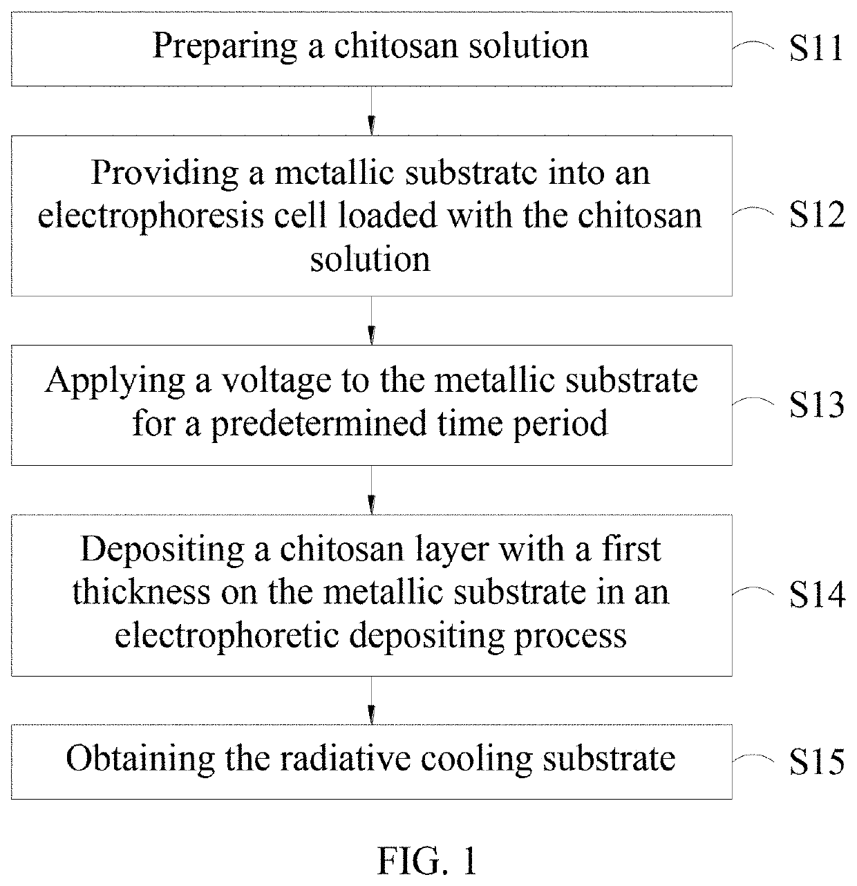
[0039]Refer to FIG. 1, which depicts a flow chart of the manufacturing method of the radiative cooling substrate according to an embodiment of the present invention.

[0040]Step S11: preparing a chitosan solution including chitosan ((C6H11O4N)n) and a solvent. Chitosan is the product after chitin is deacetylated. There is a strong correlation of the solubility of chitosan and the characteristics of the chitosan solution with the degree of deacetylation. That is, the higher the degree of deacetylation is, the more obvious ...


PUM

PropertyMeasurementUnit
thicknessaaaaaaaaaa
thicknessaaaaaaaaaa
volumeaaaaaaaaaa

Abstract

A radiative cooling substrate and a manufacturing method of the radiative cooling substrate are provided. The radiative cooling substrate includes a metallic substrate and a chitosan layer disposed on the metallic substrate with a thickness of 0.5 μm to 10 μm. The chitosan layer emits radiation within a waveband between 8 μm and 13 μm.

Description

CROSS-REFERENCE TO RELATED APPLICATION[0001]This application claims priority from Taiwan Application No. 107138663, filed on Oct. 31, 2018, in the Taiwan Intellectual Property Office, the content of which is hereby incorporated by reference in their entirety for all purposes.BACKGROUND OF THE INVENTION1. Field of the Invention[0002]The present invention relates to a radiative cooling substrate and a manufacturing method of the radiative cooling substrate. Specifically, the present invention relates to a radiative cooling substrate and a manufacturing method of the radiative cooling substrate using the passive radiation cooling effect of a deposited chitosan layer.2. Description of the Related Art[0003]Thermal energy dissipation devices are needed for various kinds of instruments, machines, and pipes in daily life for maintaining proper operation temperatures. Radiative cooling method utilizes thermal radiation as the only way for transporting thermal energy, and the velocity is iden...

Claims


Application Information

Patent Timeline
Patent Type & Authority Patents(United States)
IPC IPC(8): C25D13/06C25D13/12C25D13/20F28F13/18C25D13/22
CPCC25D13/06C25D13/12C25D13/20C25D13/22F28F13/18F28F2245/06C09D5/00C09D5/44
Inventor CHEN, YU-BINHAN, HUNG-SHENG
Owner NATIONAL TSING HUA UNIVERSITY
Learn More