Chip package structure with stacked chips and manufacturing method thereof

a technology of chip package and manufacturing method, which is applied in the direction of electrical apparatus, semiconductor devices, semiconductor/solid-state device details, etc., can solve the problems that the conventional package structure cannot meet above excellent characteristics simultaneously, and achieve the effect of reducing design time and cost, improving reliability of the chip package structure, and reducing lateral siz

Active Publication Date: 2021-09-28
YANGTZE MEMORY TECH CO LTD
View PDF15 Cites 4 Cited by
  • Summary
  • Abstract
  • Description
  • Claims
  • Application Information

AI Technical Summary

Benefits of technology

[0007]Due to the design of the chip package structure of the present invention, the chip package structure has a reduced lateral size, and the signal transmitting path between the chips of the chip package structure and the external device may be decreased. Furthermore, the design time and the cost of the chip package structure can be decreased. On the other hand, in the manufacturing process, the reliability of the chip package structure can be improved when the offset of the chip exists.

Problems solved by technology

However, the conventional package structure cannot meet above excellent characteristics simultaneously.

Method used


Image

  • Chip package structure with stacked chips and manufacturing method thereof
  • Chip package structure with stacked chips and manufacturing method thereof
  • Chip package structure with stacked chips and manufacturing method thereof

Examples


Embodiment Construction

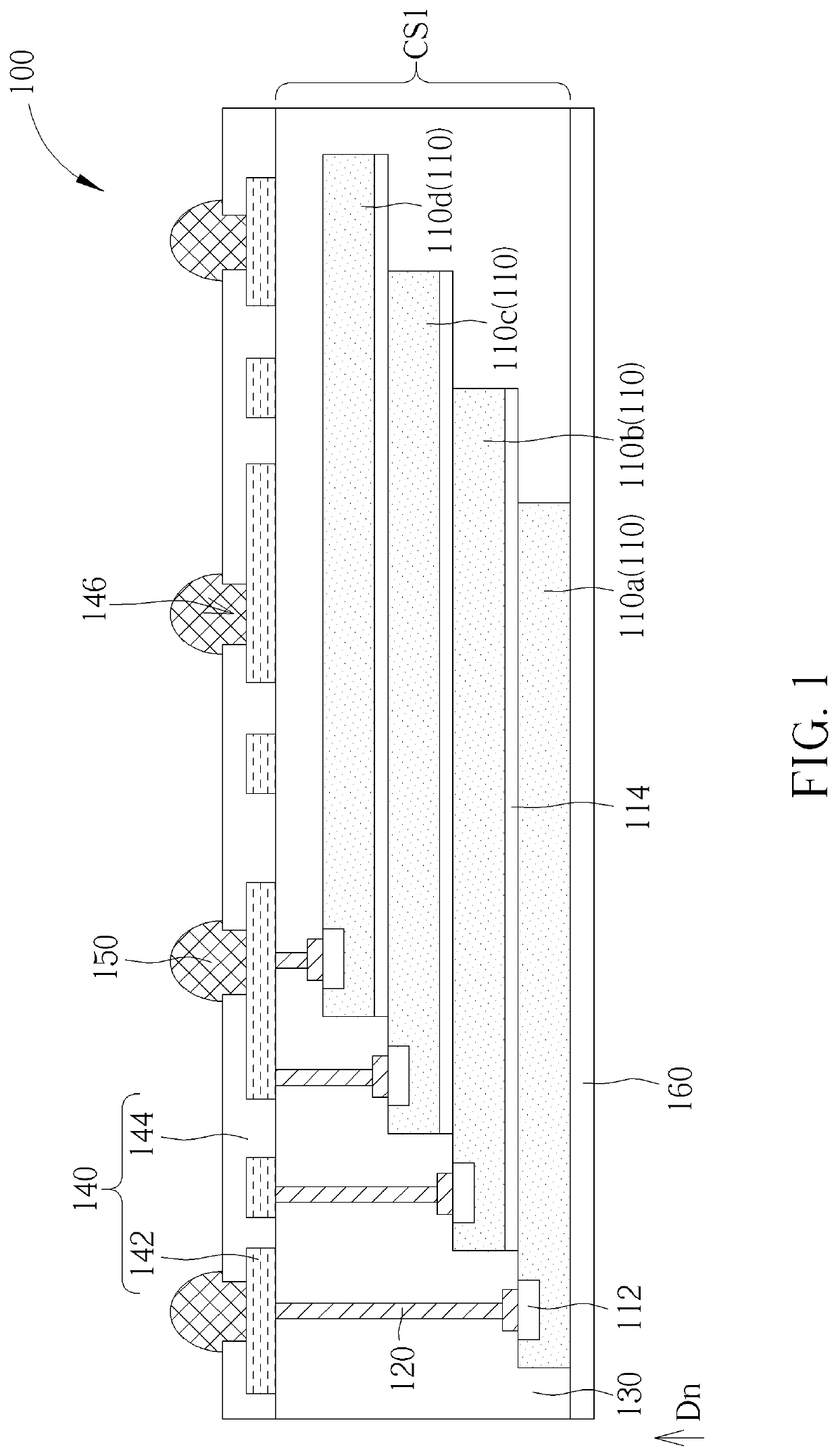
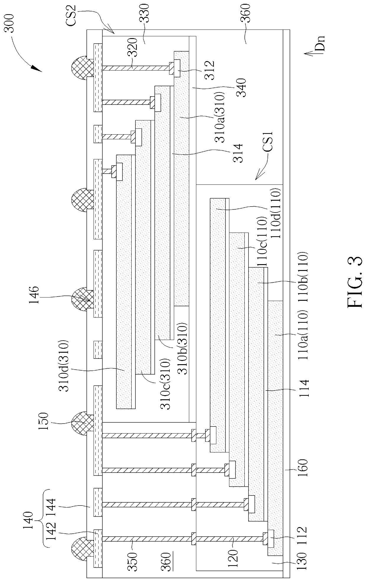
[0017]Although specific configurations and arrangements are discussed, it should be understood that this is done for illustrative purposes only. A person skilled in the pertinent art will recognize that other configurations and arrangements can be used without departing from the spirit and scope of the present disclosure. It will be apparent to a person skilled in the pertinent art that the present disclosure can also be employed in a variety of other applications.

[0018]Certain terms are used throughout the description and following claims to refer to particular components. As one skilled in the art will understand, electronic equipment manufacturers may refer to a component by different names. This document does not intend to distinguish between components that differ in name but not in function. In the following description and in the claims, the terms “include”, “comprise” and “have” are used in an open-ended fashion, and thus should be interpreted to mean “include, but not limit...


PUM


Abstract

A chip package structure including a first chip stack and a redistribution layer is provided. The first chip stack includes a plurality of first chips, a first molding layer and at least one first vertical conductive element. The plurality of first chips are sequentially stacked, wherein each of the plurality of first chips includes at least one first bonding pad, and the first bonding pads are not covered by the plurality of first chips. The first molding layer encapsulates the plurality of first chips. The at least one first vertical conductive element penetrates through the first molding layer, wherein the at least one first vertical conductive element is disposed on and electrically connected to at least one of the first bonding pads. The redistribution layer is disposed on the first chip stack and electrically connected to the at least one first vertical conductive element.

Description

CROSS REFERENCE TO RELATED APPLICATIONS[0001]This patent application is a continuation of International Application PCT / CN2019 / 121821, filed Nov. 29, 2019. The present application is based on and claims priority to International Application PCT / CN2019 / 121821 filed on Nov. 29, 2019, the contents of which are hereby incorporated by reference in their entirety.BACKGROUND OF THE INVENTION1. Field of the Invention[0002]The present invention relates to a chip package structure and a manufacturing method thereof, and more particularly to a chip package structure having a plurality of chips sequentially stacked and a manufacturing method thereof.2. Description of the Prior Art[0003]In the semiconductor fabrication process, the packaging process can encapsulate a semiconductor component, such as one or more chip(s), to form a semiconductor package structure, so as to protect the semiconductor component. Nowadays, the industries make great efforts to develop the package structure with excelle...

Claims


Application Information

Patent Timeline
Patent Type & Authority Patents(United States)
IPC IPC(8): H01L25/065H01L23/31H01L23/00H01L21/56H01L25/00H01L23/538
CPCH01L25/0657H01L21/56H01L23/3121H01L23/3135H01L23/5384H01L24/05H01L25/50H01L23/3114H01L23/49811H01L23/49838H01L23/5386H01L21/4853H01L21/76895H01L2924/181H01L2224/32145H01L23/562H01L23/3128H01L21/568H01L21/561H01L21/6835H01L2221/68345H01L2221/68372H01L2924/18162H01L2224/04105H01L2224/12105H01L2224/73267H01L2224/92244H01L2224/214H01L2224/96H01L2224/48145H01L2224/73265H01L2225/06524H01L2225/06506H01L2225/06562H01L2224/73227H01L23/5389H01L25/03H01L2224/32225H01L24/19H01L2224/45144H01L2224/45147H01L2224/45124H01L2224/45139H01L24/45H01L24/32H01L24/73H01L24/92H01L23/49816H01L2924/00012H01L2924/00014H01L2924/00
Inventor ZENG, XINRUCHEN, PENGZHOU, HOUDE
Owner YANGTZE MEMORY TECH CO LTD
Why Eureka
Try Eureka