
Method of manufacturing semiconductor integrated circuit

a manufacturing method and integrated circuit technology, applied in the direction of semiconductor devices, electrical appliances, transistors, etc., can solve the problems of difficult to secure a margin of breakdown voltage characteristic against the required design-specification

Active Publication Date: 2021-11-02
FUJI ELECTRIC CO LTD
View PDF17 Cites 0 Cited by
  • Summary
  • Abstract
  • Description
  • Claims
  • Application Information

AI Technical Summary

Benefits of technology

[0007]In view of the above-mentioned problems, an object of the invention is to provide a method of manufacturing a semiconductor integrated circuit including a plurality of multi-junction structures having opposite conductivity types, capable of improving punch-through voltages of the multi-junction structures having opposite conductivity types, which are in a trade-off relationship, and easily securing a margin of a breakdown-voltage characteristic against process variation.

Problems solved by technology

However, in a case where the p-type well region and the n-type well region are formed by a general ion implantation process and a thermal diffusion process, respectively, a punch-through voltage of the n-p-n multi-junction structure and a punch-through voltage of the p-n-p multi-junction structure is in a trade-off relationship with each other, and thus, there is a problem that it is difficult to secure a margin of breakdown-voltage characteristic against the required design-specification when the process varies.

Method used


Image

  • Method of manufacturing semiconductor integrated circuit
  • Method of manufacturing semiconductor integrated circuit
  • Method of manufacturing semiconductor integrated circuit

Examples


modified example

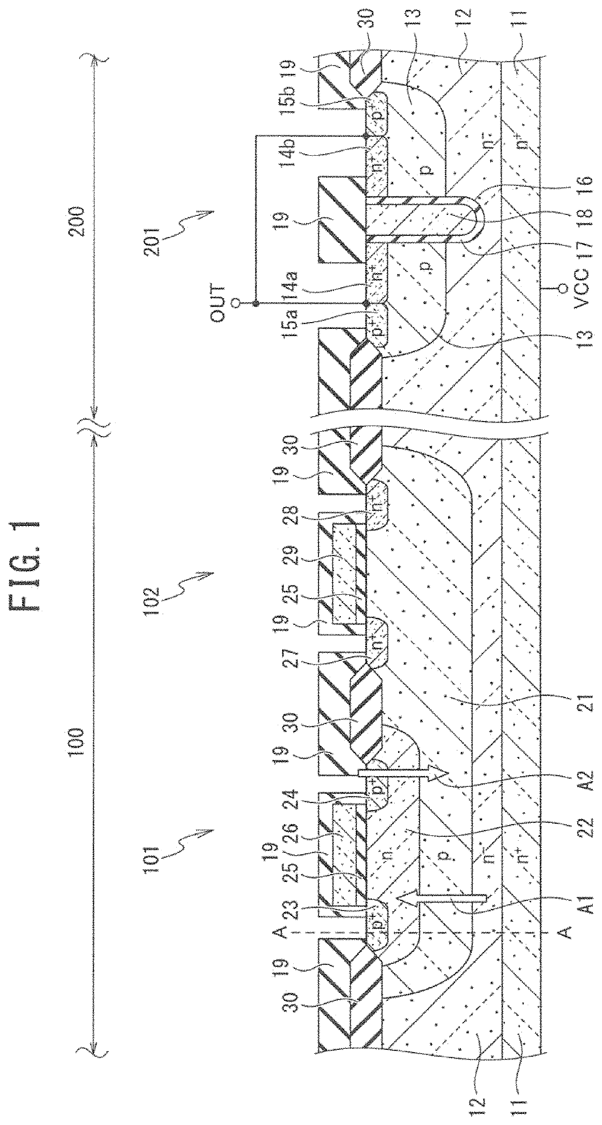
[0081]In the method of manufacturing a semiconductor integrated circuit according to the embodiment of the present invention, as illustrated in FIG. 6A, exemplified is the case of performing the thermal oxidation process after formation of the first well region 21 and before formation of the second well region 22. In contrast, absorption and extraction of the p-type impurities may be performed by forming an oxide film 35 by thermal oxidation as illustrated in FIG. 17A after formation of the second well region 22 as illustrated in FIG. 12A. In this case, the absorption and extraction of the p-type impurities may not be performed by forming an oxide film by thermal oxidation after formation of the first well region 21 and before the formation of the second well region 22.

[0082]FIG. 17B illustrates an impurity profile of the support layer 12 in the depth direction along the line A-A illustrated in FIG. 17A. As illustrated in FIG. 17B, the p-type impurities are redistributed by being ab...


PUM

PropertyMeasurementUnit
thicknessaaaaaaaaaa
breakdown-voltageaaaaaaaaaa
voltageaaaaaaaaaa

Abstract

A method of manufacturing a semiconductor integrated circuit, includes: forming a first well region having a second conductivity type in an upper portion of a support layer having a first conductivity type; forming an oxide film on the first well region by a thermal oxidation method to decrease a concentration of impurities at an top surface of top surface side of the first well region; removing the oxide film; forming a second well region having the first conductivity type in an upper portion of the first well region; and merging a semiconductor element having a main electrode region having the second conductivity type in the second well region.

Description

CROSS-REFERENCE TO RELATED APPLICATION[0001]This application claims benefit of priority under 35 USC 119 based on Japanese Patent Application No. 2018-025504 filed on Feb. 15, 2018, the entire contents of which are incorporated by reference herein.BACKGROUND OF THE INVENTION1. Field of the Invention[0002]The present invention relates to a method of manufacturing a semiconductor integrated circuit, and more particularly, to a method of manufacturing a semiconductor integrated circuit (power IC) for electric power.2. Description of the Related Art[0003]As a structural example of a high-side power IC for in-vehicle use or the like, a monolithic integrated circuit (IC) structure in which a n-channel vertical MOSFET for an output stage and a lateral MOSFET for a control circuit are built on the same n-type substrate has been known. The bottom surface side of an n-type substrate is a drain terminal of the vertical MOSFET and is connected to a power supply voltage terminal (VCC terminal) t...

Claims


Application Information

Patent Timeline
Patent Type & Authority Patents(United States)
IPC IPC(8): H01L29/66H01L27/06H01L21/8238H01L21/324H01L21/265H01L21/266H01L21/308H01L29/423H01L29/417H01L29/10H01L29/78H01L29/08H01L29/739H01L29/745
CPCH01L21/823878H01L21/266H01L21/2652H01L21/3086H01L21/324H01L21/823892H01L27/0623H01L29/0865H01L29/0882H01L29/1095H01L29/41741H01L29/42368H01L29/42376H01L29/66348H01L29/66734H01L29/7813H01L29/66363H01L29/7397H01L29/7455H01L27/0883H01L27/0922H01L21/823456H01L21/82385H01L29/36
Inventor TOYODA, YOSHIAKI
Owner FUJI ELECTRIC CO LTD
Learn More