Testing device and testing method for TFT array substrate

a thin film transistor and array substrate technology, applied in the field of display, can solve the problems of affecting the switching leakage performance of the tft device, the backlight cannot be flexibly moved, and the cost of installing the backlight is high, so as to achieve the effect of convenient operation and low cos

Active Publication Date: 2022-02-01
SHENZHEN CHINA STAR OPTOELECTRONICS SEMICON DISPLAY TECH CO LTD
View PDF7 Cites 0 Cited by
  • Summary
  • Abstract
  • Description
  • Claims
  • Application Information

AI Technical Summary

Benefits of technology

[0027]The present invention provides the following advantages: the testing device for TFT array substrate of the present invention comprises a loading platform, a test module and a driving module. The test module comprises a probe head, a connection part, a probe card, an image acquisition module and a frame, and the image acquisition module comprises a light source. When testing, the TFT array substrate is placed on the loading platform so that the test component on the TFT array substrate faces upward, and the drive module drives the frame to move the probe head, the connection portion, the probe card and the image acquisition module to move the probe card to contact the test component, the image acquisition module uses the light source to illuminate the test component, and the probe card detects the current flowing through the test component, thereby enabling photogenerated carrier interference detection on the test components at different positions on the TFT array substrate. The device has a lower cost. The testing method for TFT array substrate of the present invention can perform photogenerated carrier interference detection on every type of TFT array substrate, and is easy to operate.

Problems solved by technology

When the LCD is in operation, since the backlight module emits a backlight to the LCD panel, the TFT device on the TFT array substrate is irradiated by the backlight to generate photogenerated carriers, which affects the switching leakage performance of the TFT device.
However, in this design, the cost of installing the backlight is high, and at the same time, the backlight cannot be flexibly moved, which would easily cause the problem that the test components at certain positions on the TFT array substrate are not located above the backlight, and the photogenerated carrier operation environment cannot be effectively realized.
Also, because the distribution of test components on different types of TFT array substrates is quite different, the fixed backlight cannot meet the testing requirements of different TFT array substrates.

Method used


Image

  • Testing device and testing method for TFT array substrate
  • Testing device and testing method for TFT array substrate
  • Testing device and testing method for TFT array substrate

Examples


Embodiment Construction

[0032]To further explain the technical means and effect of the present invention, the following refers to embodiments and drawings for detailed description. Apparently, the described embodiments are merely some embodiments of the present invention, instead of all embodiments. All other embodiments based on embodiments in the present invention and obtained by those skilled in the art without departing from the creative work of the present invention are within the scope of the present invention.

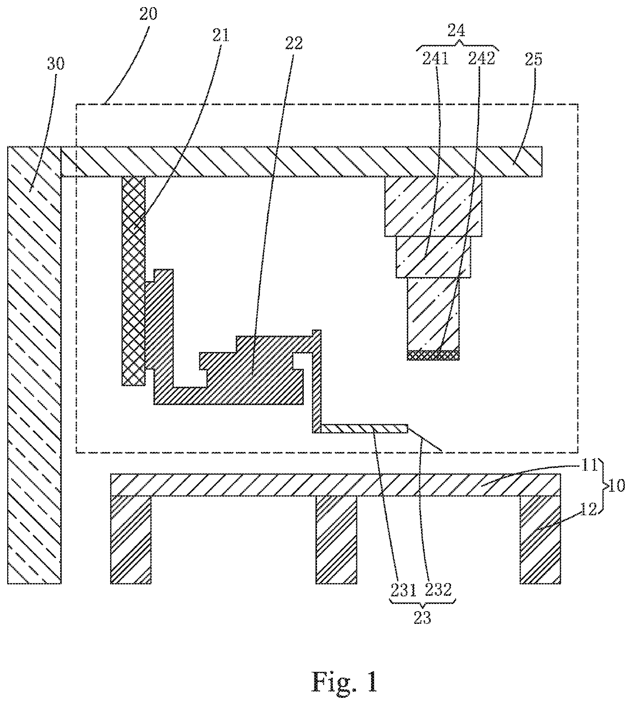
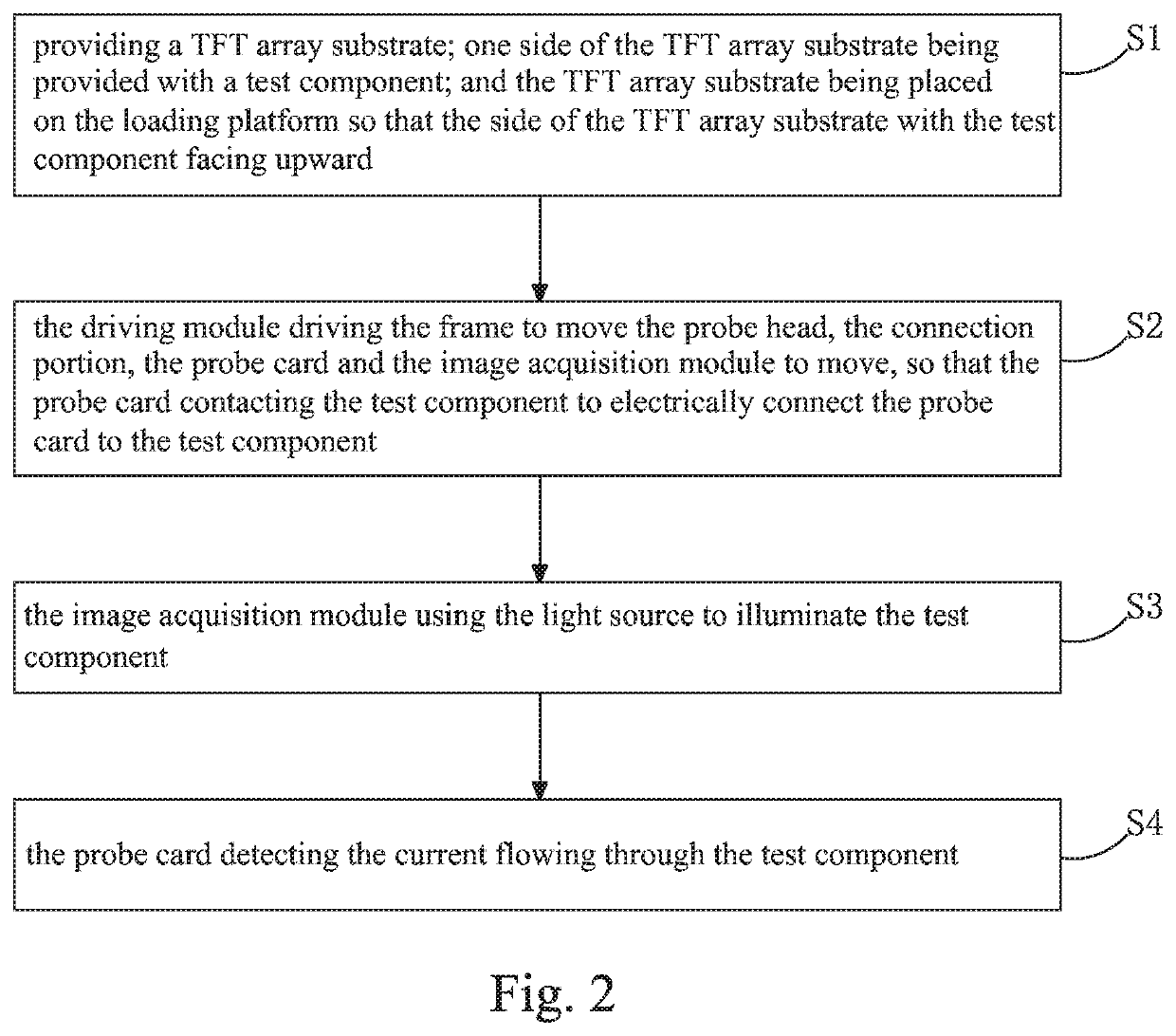
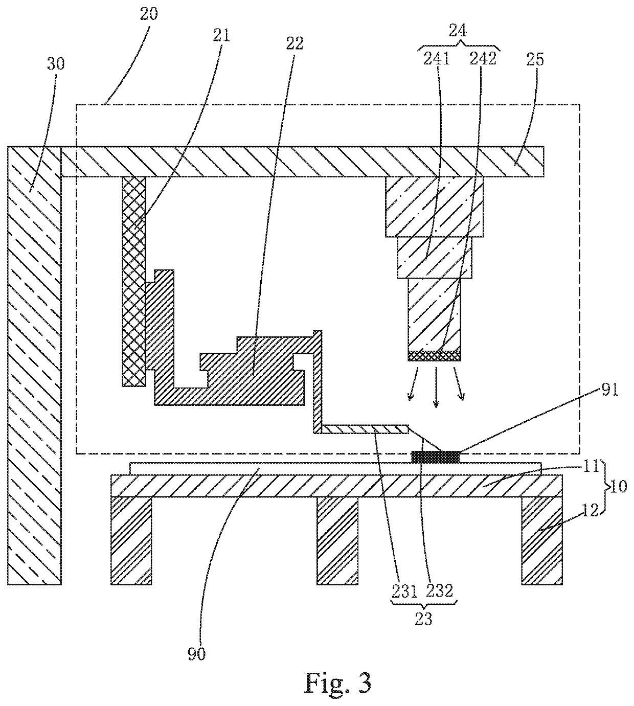
[0033]Refer to FIG. 1. The testing device for TFT array substrate of the present invention comprises: a loading platform 10, a test module 20 disposed above the loading platform 10, and a driving module 30 connected to the test module 20.

[0034]The test module 20 comprises a vertical probe head 21 disposed above the loading platform 10, a connection portion 22 disposed on one side of the probe head 21, a probe card 23 disposed at a side of the connection portion 22 away from the probe head 21, a...


PUM

PropertyMeasurementUnit
driving voltageaaaaaaaaaa
areaaaaaaaaaaa
currentaaaaaaaaaa

Abstract

Apparatus for testing microelectronic components on a substrate, including a scanner operative to scan a light beam over a plurality of thin film transistors disposed on a substrate, one transistor at a time, so as to induce a photoconductive response in the plurality of transistors, one transistor at a time; current sensing circuitry operative, synchronously with said scanner, to measure an output induced by the photoconductive response associated with a transistor and to generate photoconductive response output values, the photoconductive response output values representing a photoconductive response induced by the light beam, for one transistor at a time from among the plurality of transistors; and diagnostic apparatus operative to analyze the electronic response output values and to characterize each of the transistors in accordance therewith.

Description

BACKGROUND OF THE INVENTION1. Field of the Invention[0001]The present invention relates to the field of display and, in particular, to the field of a testing device and testing method for thin film transistor (TFT) array substrate.2. The Related Arts[0002]As the display technologies progress, the liquid crystal display (LCD) and the organic light-emitting diode (OLED) display, with many advantages such as high image quality, power saving, thinness and wide application range, are widely used in various consumer electronic products such as mobile phones, televisions, personal digital assistants, digital cameras, notebook computers, desktop computers, and so on, and have become the mainstream in the display device.[0003]Most of the LCDs on the existing market are backlight type LCD, which comprises an LCD panel and a backlight module. The working principle of the LCD panel is to fill liquid crystal (LC) molecules between a TFT array substrate and a color filter (CF) substrate, and appl...

Claims


Application Information

Patent Timeline
Patent Type & Authority Patents(United States)
IPC IPC(8): G01R31/28G01R31/311
CPCG01R31/2887G01R31/2893G01R31/311G09G3/006
Inventor ZHENG, YALAN
Owner SHENZHEN CHINA STAR OPTOELECTRONICS SEMICON DISPLAY TECH CO LTD
Why Eureka
Try Eureka