Supercharge Your Innovation With Domain-Expert AI Agents!

Semiconductor package

a technology of semiconductors and components, applied in the structural form of radiating elements, protection material radiating elements, basic electric elements, etc., can solve the problems of critical safety issues and deterioration of electronic devices performan

Active Publication Date: 2022-02-01
SAMSUNG ELECTRONICS CO LTD +1
View PDF17 Cites 1 Cited by
  • Summary
  • Abstract
  • Description
  • Claims
  • Application Information

AI Technical Summary

Benefits of technology

The present invention provides a semiconductor package with improved efficiency and reliability. The package includes a substrate with substrate patterns that cover most of the substrate surface. The substrate patterns can include antenna patterns, which improve signal transmission and stability. The package also includes solder bumps, a shielding layer, a redistribution layer, and vias for grounding and power. The redistribution layer is electrically connected to the semiconductor chip, and the shielding layer protects it from external interference. These features make the semiconductor package more reliable and efficient for use in various electronic devices.

Problems solved by technology

However, electromagnetic waves emitted from the electronic device may deteriorate performance of the electronic device.
For example, the electromagnetic waves may cause malfunction of a communication device such that critical safety issues may be generated.

Method used


Image

  • Semiconductor package
  • Semiconductor package
  • Semiconductor package

Examples


Embodiment Construction

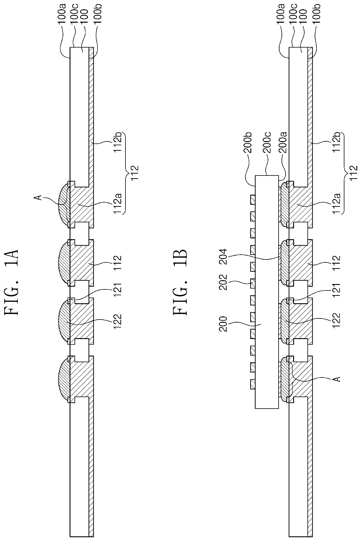
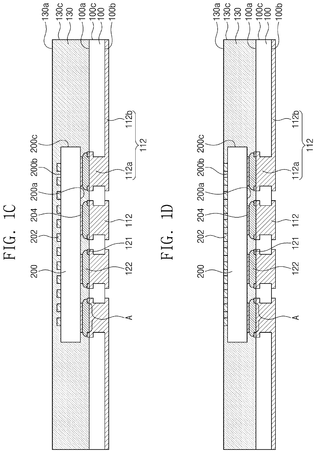
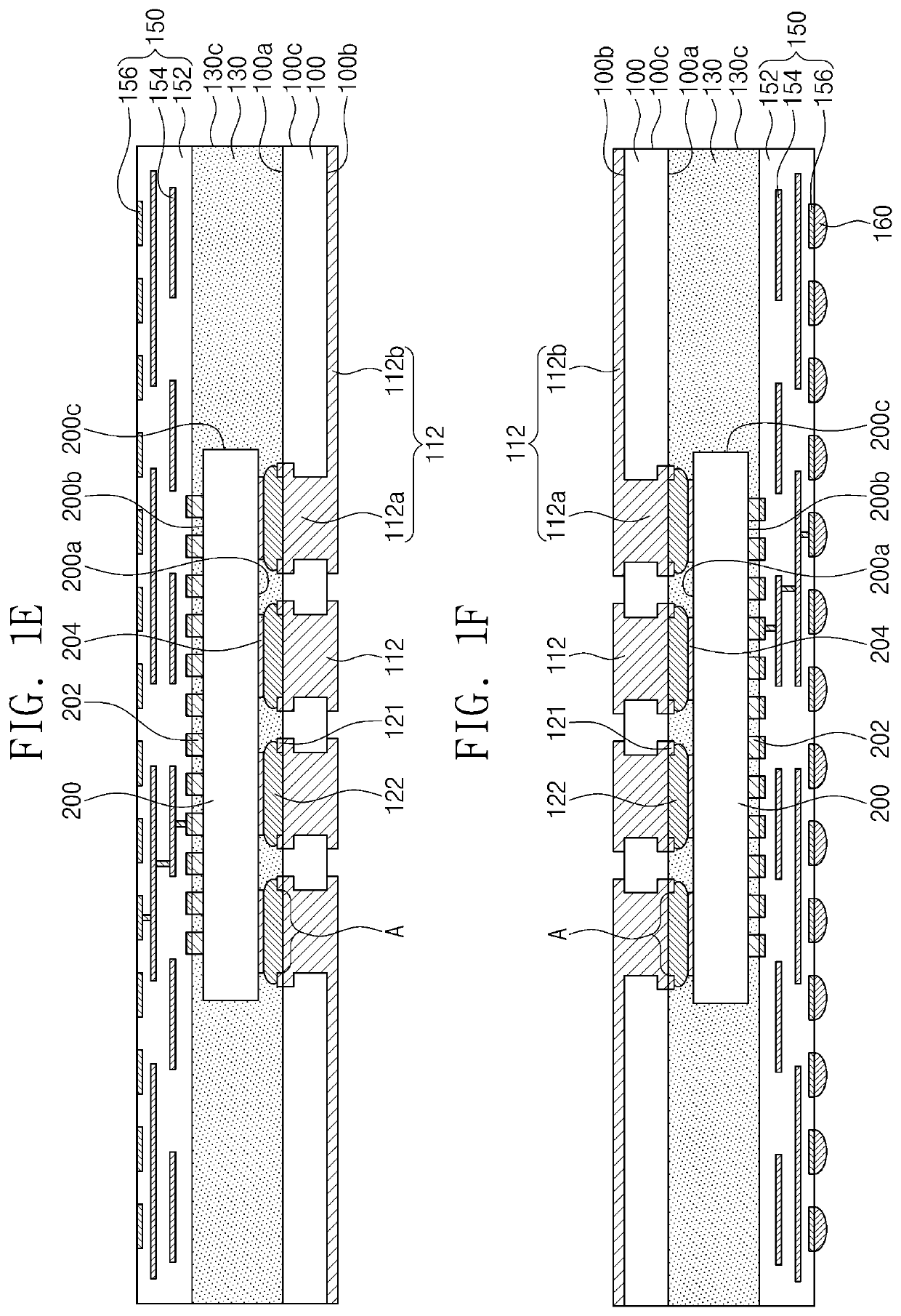
[0014]The same reference numerals or the same reference designators may denote the same elements or components throughout the specification and the drawings. Semiconductor packages and methods for manufacturing the sane according to an exemplary embodiment of the present inventive concept will be described hereinafter.

[0015]FIGS. 1A, 1B, 1C, 1D, 1E and 1F are cross-sectional views illustrating a method for manufacturing a semiconductor package according to an exemplary embodiment of the present inventive concept.

[0016]Referring to FIG. 1A, a substrate 100 may be prepared. The substrate 100 may be a printed circuit board (PCB). For example, the substrate 100 may be a metal thin plate including an insulating layer. The substrate 100 may have a first surface 100a and a second surface 100b. The substrate 100 may be prepared with substrate patterns 112 provided therein. The substrate patterns 112 may vertically penetrate the substrate 100 and may be exposed at a top surface (e.g., the fi...


PUM

PropertyMeasurementUnit
total areaaaaaaaaaaa
shapesaaaaaaaaaa
widthaaaaaaaaaa

Abstract

A semiconductor package includes: a substrate; a semiconductor chip disposed on a first surface of the substrate; solder bumps disposed between a first surface of the semiconductor chip and the substrate; and a redistribution layer provided on a second surface, opposite to the first surface, of the semiconductor chip. The substrate includes substrate patterns, and the substrate patterns cover a second surface of the substrate. The substrate patterns cover 60% to 100% of a total area of the second surface of the substrate.

Description

CROSS-REFERENCE TO RELATED APPLICATION[0001]This U.S. non-provisional patent application claims priority under 35 U.S.C. § 119 to Korean Patent Application No. 10-2019-0074185, filed on Jun. 21, 2019, in the Korean Intellectual Property Office, the disclosure of which is incorporated by reference herein in its entirety.TECHNICAL FIELD[0002]Exemplary embodiments of the present inventive concept relate to a semiconductor package and, more particularly, to a semiconductor package having an electromagnetic shielding function and an antenna function.DISCUSSION OF THE RELATED ART[0003]A packaging density may be increased to increase speed and provide miniaturization of an electronic device. However, electromagnetic waves emitted from the electronic device may deteriorate performance of the electronic device. For example, the electromagnetic waves may cause malfunction of a communication device such that critical safety issues may be generated. Thus, electromagnetic shielding techniques fo...

Claims


Application Information

Patent Timeline
Patent Type & Authority Patents(United States)
IPC IPC(8): H01L23/538H01L23/552H01L23/66H01L23/00H01L21/48H01L21/56H01Q1/38H01L23/31
CPCH01L23/5389H01L21/4853H01L21/4857H01L21/565H01L23/3128H01L23/5383H01L23/5386H01L23/552H01L23/66H01L24/19H01L24/20H01Q1/38H01L2223/6672H01L2224/214H01L2924/3025H01Q1/2283H01L2223/6677H01Q9/0414H01Q21/065H01Q1/40H01L23/49827H01L23/49833H01L2224/73259H01L2224/16235H01L2224/92224H01L2224/12105H01L2224/04105H01L2224/0401H01L2224/81192H01L2224/05647H01L2224/05166H01L2224/05073H01L24/13H01L24/05H01L2224/0391H01L2224/17106H01L24/16H01L2224/05557H01L24/17H01L24/24H01L2224/24227H01L2224/131H01L2924/00014H01L2924/014H01L23/62H01L23/525H01L23/481H01L24/14H01L23/31
Inventor KIM, YOUNG-HOPARK, HWAN PILKIM, SUNG-CHULAHN, KEY-ONE
Owner SAMSUNG ELECTRONICS CO LTD
Features
  • R&D
  • Intellectual Property
  • Life Sciences
  • Materials
  • Tech Scout
  • Unparalleled Data Quality
  • Higher Quality Content
  • 60% Fewer Hallucinations
Learn More