Flexible display panel and flexible display device
a display panel and flexible technology, applied in the field of flexible display, can solve the problems of affecting the optical effect of the amoled screen, tin oxide is used as a brittle semiconductor material, and is not suitable for application for flexible display screen, so as to improve the overall display effect of the display area, reduce the arrangement density of metal traces, and improve the effect of light emitted by sub pixels
- Summary
- Abstract
- Description
- Claims
- Application Information
AI Technical Summary
Benefits of technology
Problems solved by technology
Method used
Image
Examples
first embodiment
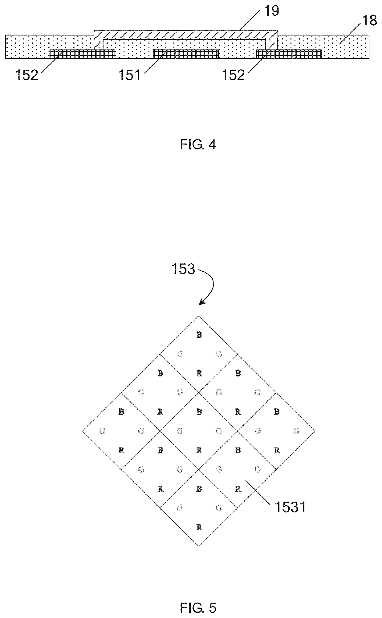
[0056]Please refer to FIG. 5. FIG. 5 is a structural diagram of a touch electrode according to the present invention. As an optional implementation, as shown in FIG. 5, at least one of the touch electrodes 153 comprises nine first touch areas 1531. Each of the first touch areas 1531 is correspondingly arranged with two green sub pixels G, one red sub pixel R and one blue sub pixel B. The two green sub pixels G, one red sub pixel R and one blue sub pixel B located in each of the first touch areas 1531 shown in FIG. 5 constitute one GRGB pixel unit. In other embodiments, the number and arrangement of the sub pixels corresponding to the first touch area 1531 are not limited thereto.
second embodiment
[0057]As another optional implementation, a number of sub pixels correspondingly arranged in a portion of the plurality of first touch areas 1531 is the same as shown in FIG. 6. Please refer to FIG. 6, FIG. 6 is a structural diagram of a touch electrode according to the present invention. As an optional implementation, as shown in FIG. 6, at least one of the touch electrodes 153 comprises six first touch areas 1531. The five first touch areas 1531 is correspondingly arranged with one GRGB pixel unit and one of the first touch areas 1531 is correspondingly arranged with four GRGB pixel units.
[0058]Please refer to FIG. 7 and FIG. 8. FIG. 7 is a structural diagram of a touch electrode according to the third embodiment of the present invention. FIG. 8 is a structural diagram of a touch electrode according to the fourth embodiment of the present invention. As an optional implementation, as shown in FIG. 7 or FIG. 8, at least one of the touch electrodes 153 comprises three first touch are...
fifth embodiment
[0061]Please refer to FIG. 9. FIG. 9 is a structural diagram of a touch electrode according to the present invention. As an optional implementation, as shown in FIG. 9, at least one of the touch electrodes 153 comprises six first touch areas 1531 and twelve second touch areas 1532. Each of the first touch areas 1531 is correspondingly arranged with one of the GRGB pixel units. It can be understood that the arrangements of the first touch areas 1531 and the second touch areas 1532 of the present invention are not limited to the arrangement shown in FIG. 9, and any other arrangements may be used. The repeated description is omitted here.
[0062]In one another specific embodiment, at least one of the touch electrodes 153 comprises only a plurality of the second touch areas 1532.
PUM
| Property | Measurement | Unit |
|---|---|---|
| width | aaaaa | aaaaa |
| width | aaaaa | aaaaa |
| flexible | aaaaa | aaaaa |
Abstract
Description
Claims
Application Information


