Gan rectifier suitable for operating under 35GHZ alternating-current frequency, and preparation method therefor

a rectifier and alternating current technology, applied in the field of rectifiers, can solve the problems of large device volume, large reverse leakage current, serious heating under high and medium-frequency operations, etc., and achieve the effect of high degree of matching and easy implementation

Active Publication Date: 2022-02-22
SOUTH CHINA UNIV OF TECH
View PDF9 Cites 0 Cited by
  • Summary
  • Abstract
  • Description
  • Claims
  • Application Information

AI Technical Summary

Benefits of technology

[0004]In order to overcome the disadvantages and shortcomings of the prior art, it is an objective of the present invention to provide a method for preparing a GaN rectifier suitable for operating at an alternating current frequency of 35 GHz. The method has the advantages of a high degree of matching with the existing production means in preparation and being easy to implement.
[0034](1) The present invention makes it possible to prepare a high-frequency (35 GHz) GaN rectifier, in which a T-shaped gate design is adopted in the schottky contact electrode structure design part, and can effectively improve the rectifier device gate-controlled properties and effectively reduce the current concentration effect of the rectifier device during operation, improve the performance stability of the rectifier device under high power operation.
[0035](2) According to the present invention, group III nitride, such as GaN as a representative, is used as the basic material of the rectifier. Compared with traditional Si material, relying on the better material characteristics of group III nitride, the present invention can better realize miniaturization and integration of the device in higher frequency applications.
[0036](3) According to the present invention, n-polar group III nitride is used as the substrate material of the device, and compared with the traditional metal polarity surface group III nitride, the present invention can effectively enhance the two-dimensional electronic gas confinement at the interface of AlGaN / GaN heterojunction and enhance the gate-controlled properties of the device, thereby making it easy to produce enhanced rectifier devices suitable for operating at an alternating current frequency of 35 GHz.

Problems solved by technology

Traditional Si-based rectifier thyristors, because of narrow band gap, low electronic saturated migration rate, low thermal conductivity or the like of their materials, cause large device volume, large reverse leakage current, serious heating under high and medium-frequency operations and other performance stability problems.
It is thus difficult to meet the increasing requirements for device miniaturization, integration and high frequency.

Method used


Image

  • Gan rectifier suitable for operating under 35GHZ alternating-current frequency, and preparation method therefor
  • Gan rectifier suitable for operating under 35GHZ alternating-current frequency, and preparation method therefor

Examples


embodiment 1

[0042]A method for preparing a GaN rectifier chip suitable for operating at an alternating current frequency of 35 GHz on a silicon substrate of this embodiment is as follows.

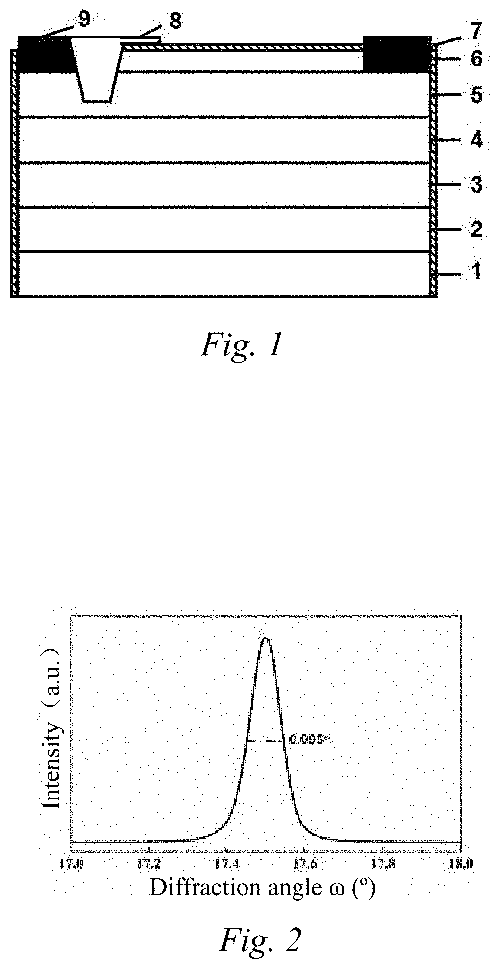
[0043](1) As shown in FIG. 1, by using metal organic chemical vapor deposition technique, a GaN rectifier epitaxial wafer is grown on a silicon substrate, including an N-polar GaN buffer layer 2 grown on the silicon substrate 1, a carbon doped semi-insulated N-polar GaN layer 3 grown on the N-polar GaN buffer layer 2 with the doping concentration of 5.9×1018 cm−3, a non-doped N-polar AlGaN layer 4 grown on the carbon doped semi-insulated N-polar GaN layer 3, a non-doped N-polar GaN layer 5 grown on the non-doped N-polar AlGaN layer 4, a non-doped N-polar InGaN thin film 6 grown on the non-doped N-polar GaN layer 5, wherein the GaN buffer layer is 800 nm in thickness; the carbon doped GaN layer 4 is 100 nm in thickness; the non-doped AlGaN layer is 450 nm in thickness; the non-doped GaN layer is 500 nm in thickn...

embodiment 2

[0060]A method for preparing a GaN rectifier chip suitable for operating at an alternating current frequency of 35 GHz on a silicon substrate of this embodiment is as follows.

[0061](1) By using metal organic chemical vapor deposition technique, a GaN rectifier epitaxial wafer is grown on a silicon substrate, including an N-polar GaN buffer layer grown on the silicon substrate, a carbon doped semi-insulated N-polar GaN layer grown on the N-polar GaN buffer layer with the doping concentration of 5.9×1018 cm−3, a non-doped N-polar AlGaN layer grown on the carbon doped semi-insulated N-polar GaN layer, a non-doped N-polar GaN layer grown on the non-doped N-polar AlGaN layer, a non-doped N-polar InGaN thin film grown on the non-doped N-polar GaN layer, wherein the GaN buffer layer is 600 nm in thickness; the carbon doped GaN layer is 150 nm in thickness. the non-doped AlGaN layer is 300 nm in thickness; the non-doped GaN layer is 400 nm in thickness; and the non-doped InGaN layer is 70 n...

embodiment 3

[0078]A method for preparing a GaN rectifier chip suitable for operating at an alternating current frequency of 35 GHz on a silicon substrate of this embodiment is as follows.

[0079](1) By using metal organic chemical vapor deposition technique, a GaN rectifier epitaxial wafer is grown on a silicon substrate, including an N-polar GaN buffer layer grown on the silicon substrate, a carbon doped semi-insulated N-polar GaN layer grown on the N-polar GaN buffer layer with the doping concentration of 5.9×1018 cm−3, a non-doped N-polar AlGaN layer grown on the carbon doped semi-insulated N-polar GaN layer, a non-doped N-polar GaN layer grown on the non-doped N-polar AlGaN layer, a non-doped N-polar InGaN thin film grown on the non-doped N-polar GaN layer, wherein the GaN buffer layer is 850 nm in thickness; the carbon doped GaN layer is 200 nm in thickness; the non-doped AlGaN layer is 450 nm in thickness; the non-doped GaN layer is 650 nm in thickness; and the non-doped InGaN layer is 150 ...


PUM

PropertyMeasurementUnit
alternating current frequencyaaaaaaaaaa
timeaaaaaaaaaa
timeaaaaaaaaaa

Abstract

The present invention discloses a method for preparing a GaN rectifier suitable for operating at an alternating current frequency of 35 GHz: sequentially growing, on a silicon substrate, an N-polar GaN buffer layer, a carbon doped semi-insulated N-polar GaN layer, a non-doped N-polar AlGaN layer, a non-doped N-polar GaN layer and a non-doped N-polar InGaN thin film to obtain a rectifier epitaxial wafer; preparing a pattern groove for a schottky contact electrode on the GaN rectifier epitaxial wafer, and depositing the schottky contact electrode in the groove; preparing a pattern for an ohmic contact electrode, and depositing a device ohmic contact electrode on the surface of the epitaxial wafer; subsequently, depositing a silicon nitride passivation layer at a part where there is no electrode on the surface of the epitaxial wafer, and preparing a surface electrode area; and finally, performing mesa isolation treatment on the GaN rectifier epitaxial wafer. The present invention realizes the preparation of a high-frequency GaN rectifier, and improves the performance stability of a rectifier device operating at a high power.

Description

CROSS-REFERENCE TO RELATED APPLICATIONS[0001]This application is the U.S. national stage of International Patent Application No. PCT / CN2018 / 074684, filed on Jan. 31, 2018 and entitled GAN RECTIFIER SUITABLE FOR OPERATING UNDER 35 GHZ ALTERNATING-CURRENT FREQUENCY, AND PREPARATION METHOD THEREFOR, which claims the benefit of priority under 35 U.S.C. § 119 from Chinese Patent Application No. 201711351659.1, filed Dec. 15, 2017. The disclosures of the foregoing applications are incorporated herein by reference in their entirety.TECHNICAL FIELD[0002]The present invention relates to a rectifier, particularly a GaN rectifier suitable for operating at an alternating current frequency of 35 GHz, and to a preparation method therefor.BACKGROUND ART[0003]A rectifier that is used as a power electronic component which plays an important role in the fields of national defense, energy transmission, etc. is of a concern to various industries. Traditional Si-based rectifier thyristors, because of na...

Claims


Application Information

Patent Timeline
Patent Type & Authority Patents(United States)
IPC IPC(8): H01L29/15H01L29/66H01L21/02H01L21/3065H01L29/20H01L29/812
CPCH01L29/66856H01L21/0254H01L21/02381H01L21/02433H01L21/02609H01L21/3065H01L29/2003H01L29/812H01L27/04H01L29/10H01L29/20H01L29/66227H01L29/66984H01L29/872H01L29/205H01L29/475H01L29/66212H01L23/3185
Inventor WANG, WENLIANGLI, GUOQIANGLI, XIAOCHANLI, YUAN
Owner SOUTH CHINA UNIV OF TECH
Why Eureka
Try Eureka