

Evaluation method and manufacturing method of SiC epitaxial wafer
a manufacturing method and epitaxial wafer technology, applied in the direction of semiconductor/solid-state device testing/measurement, fluorescence/phosphorescence, instruments, etc., can solve the problems of stacking faults, bpds in the sic substrate being converted into teds, and reducing device reliability
- Summary
- Abstract
- Description
- Claims
- Application Information
AI Technical Summary
Benefits of technology
Problems solved by technology
Method used
Image

Examples
Embodiment Construction
[0040]Hereinafter, an embodiment of the present invention will be described in detail with reference to the drawings as appropriate. In the drawings used in the following description, for ease of understanding of the features of the present invention, there are cases where characteristic portions are enlarged for convenience, and the dimension, the ratio and the like of each constituent element may be the same or may be different from reality. The materials, dimensions, and the like shown in the following description are merely examples, and the present invention is not limited thereto and can be embodied in appropriately modified manners in a range that does not change the gist thereof.
[0041]“Manufacturing Method of SiC Epitaxial Wafer”
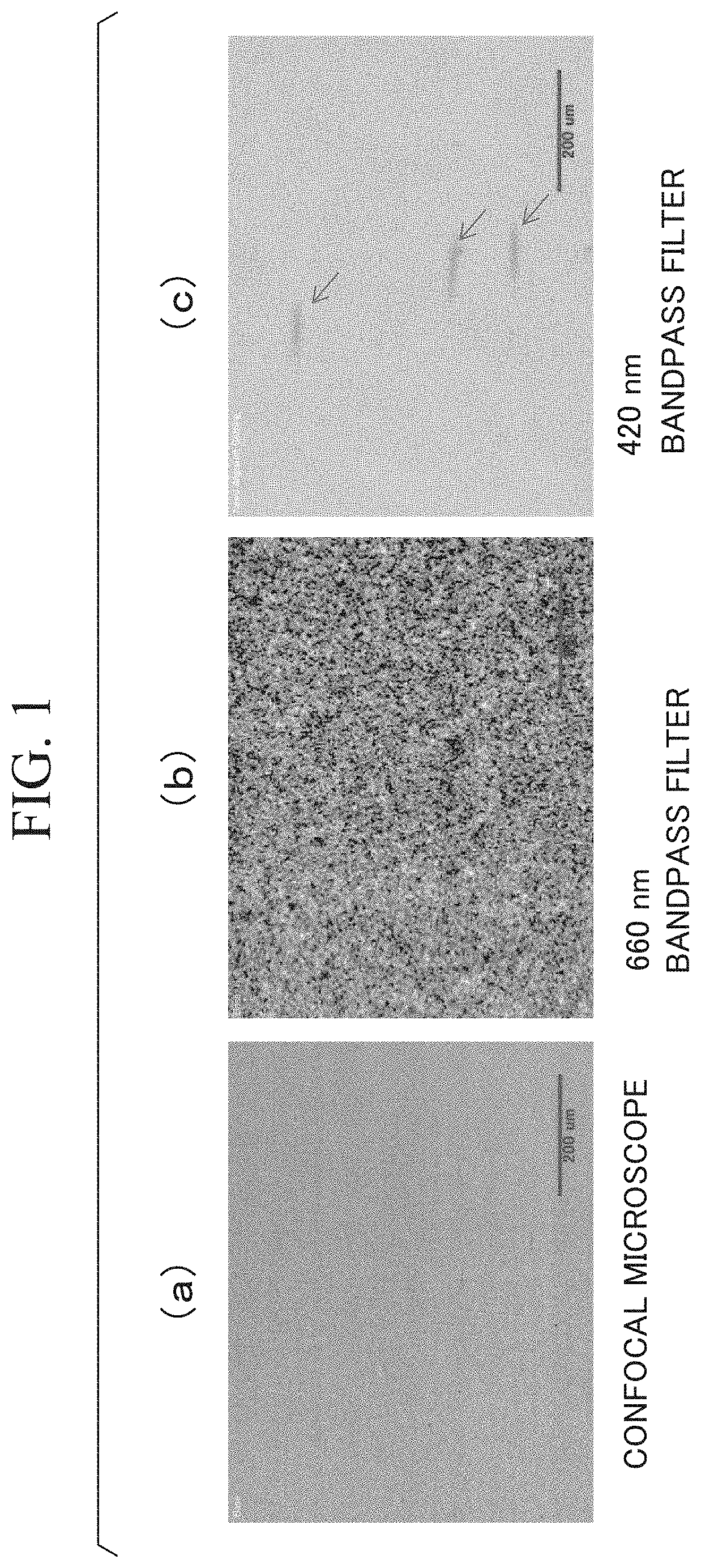
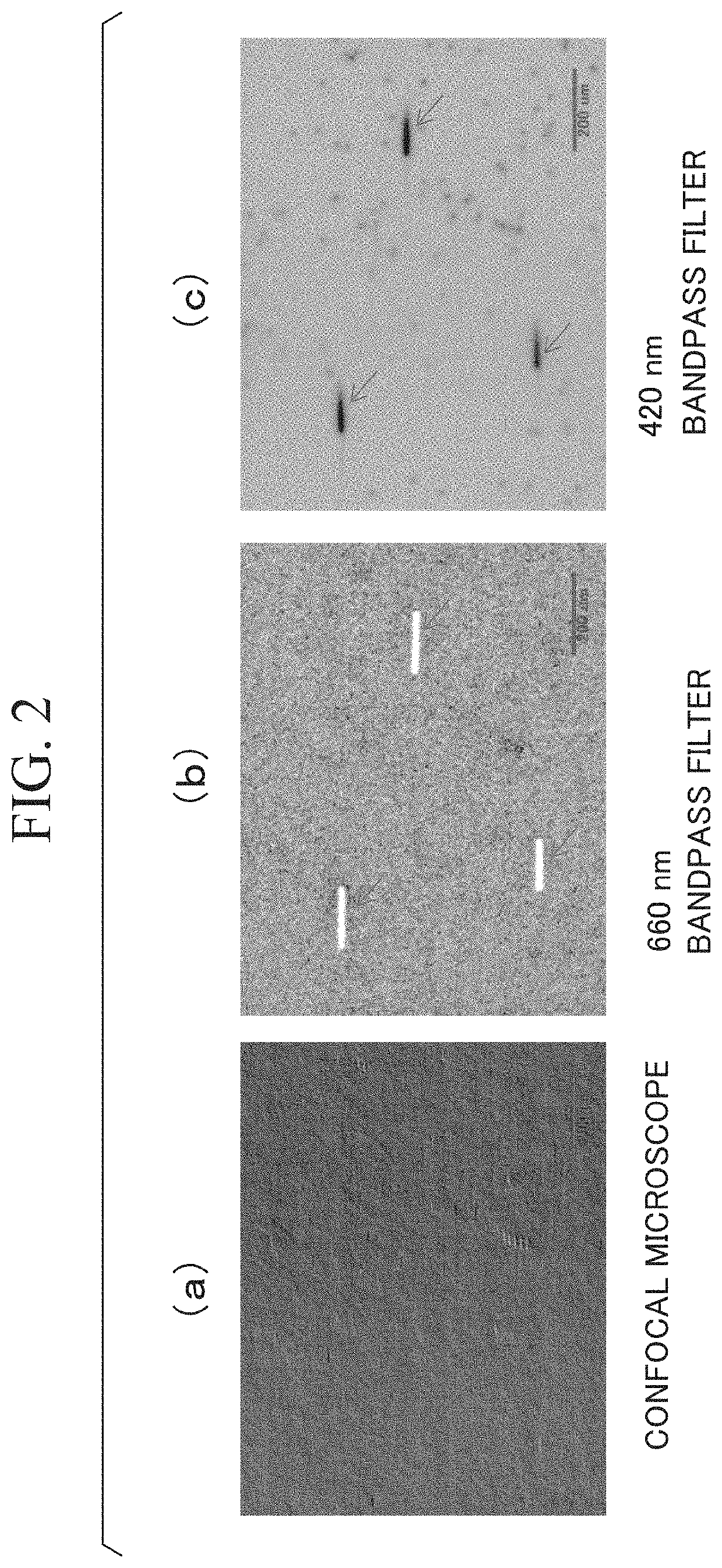
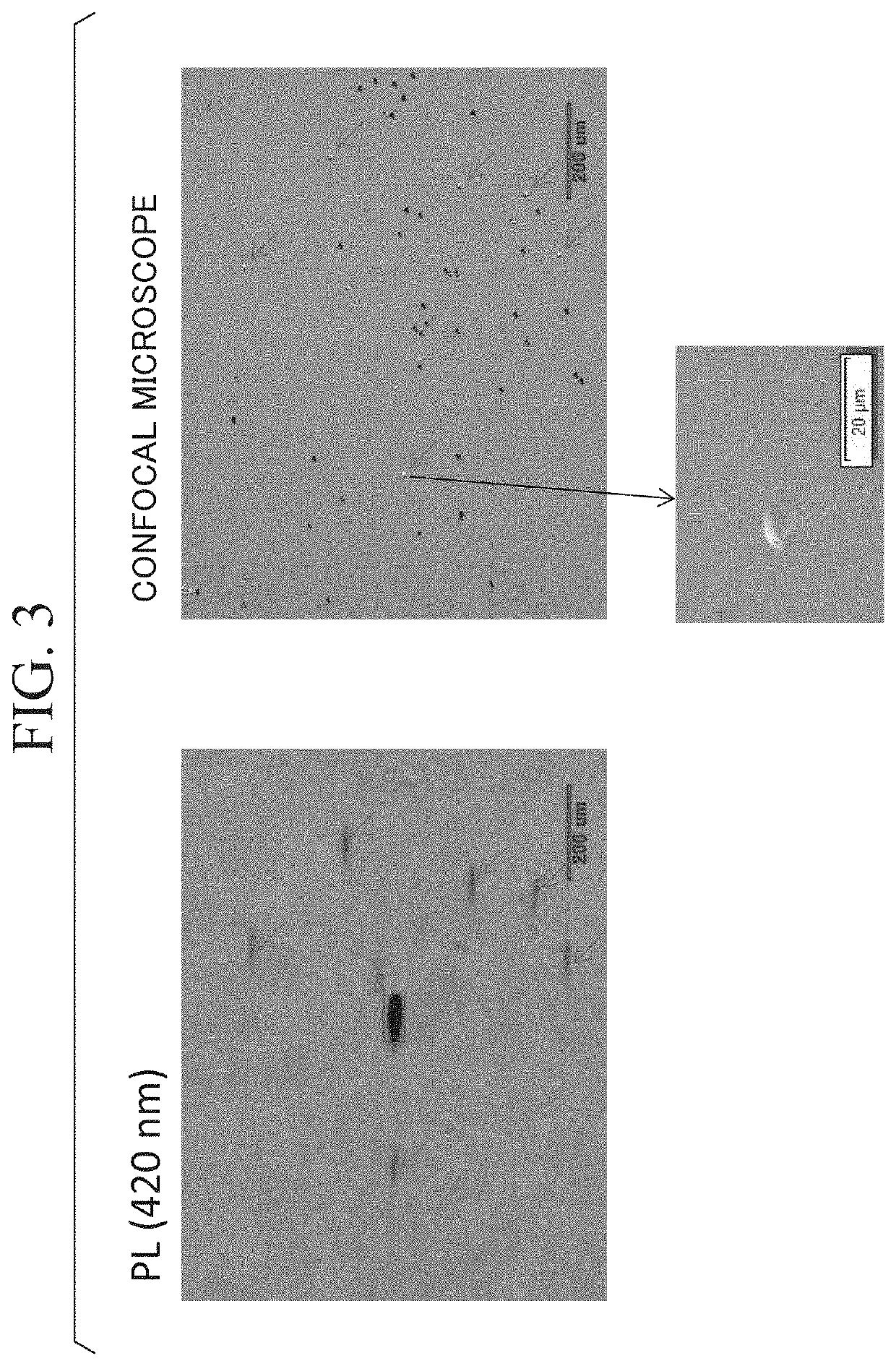
[0042]A manufacturing method of a SiC epitaxial wafer according to the embodiment includes a step of stacking a high-concentration epitaxial layer having an impurity concentration of 1×1018 cm−3 or more on a SiC substrate, a step of evaluating the hi...
PUM
| Property | Measurement | Unit |
|---|---|---|
| wavelength band | aaaaa | aaaaa |
| aspect ratio | aaaaa | aaaaa |
| wavelength band | aaaaa | aaaaa |
Abstract
Description
Claims
Application Information