Ceramic wiring board and method for producing the same

a wiring board and ceramic technology, applied in the direction of printed circuit, printed element electric connection formation, conductive pattern formation, etc., can solve the problem of difficulty in plating and mounting electrodes

Active Publication Date: 2022-05-31
MURATA MFG CO LTD
View PDF20 Cites 0 Cited by
  • Summary
  • Abstract
  • Description
  • Claims
  • Application Information

AI Technical Summary

Benefits of technology

[0011]In an unfired ceramic wiring board that includes an unfired ceramic insulator and unfired via-conductors, an amorphous constituent of the unfired ceramic insulator and an amorphous constituent of the unfired via-conductors commonly have a high affinity for each other. This causes the amorphous constituent of the unfired ceramic insulator to migrate into the unfired via-conductors in the process of firing of the unfired ceramic wiring board. Thus, even when the content of the amorphous constituent in portions of the unfired via-conductors which are located in the vicinity of the surface of the unfired ceramic wiring board is reduced, the migration of the amorphous constituent from the unfired ceramic insulator increases the content of the amorphous constituent in the above portions of the unfired via-conductors. As a result, the amorphous constituent may rise to the end portions of the via-conductors as in the related art.
[0070]In the method for producing a ceramic wiring board according to the present invention, a crystalline constituent is precipitated in the amorphous constituent when the unfired ceramic wiring board is fired. This reduces the amount of residual amorphous constituent and increases the viscosity of the amorphous constituent at high temperatures. As a result, the likelihood of the amorphous constituent rising to the end portion of the via-conductor can be limited. Furthermore, the ions of the metal element constituting the oxide included in the via-conductor are diffused into the amorphous constituent of the ceramic insulator. This improves the bond between the via-conductor and the ceramic insulator and reduces the likelihood of the via-conductor detaching from the ceramic insulator.

Problems solved by technology

This makes it difficult to form the mounting electrodes by plating.

Method used


Image

  • Ceramic wiring board and method for producing the same
  • Ceramic wiring board and method for producing the same
  • Ceramic wiring board and method for producing the same

Examples


Embodiment Construction

[0082]The features of the present invention are described more in detail with reference to embodiments of the present invention.

[0083]—Ceramic Wiring Board According to One Embodiment—

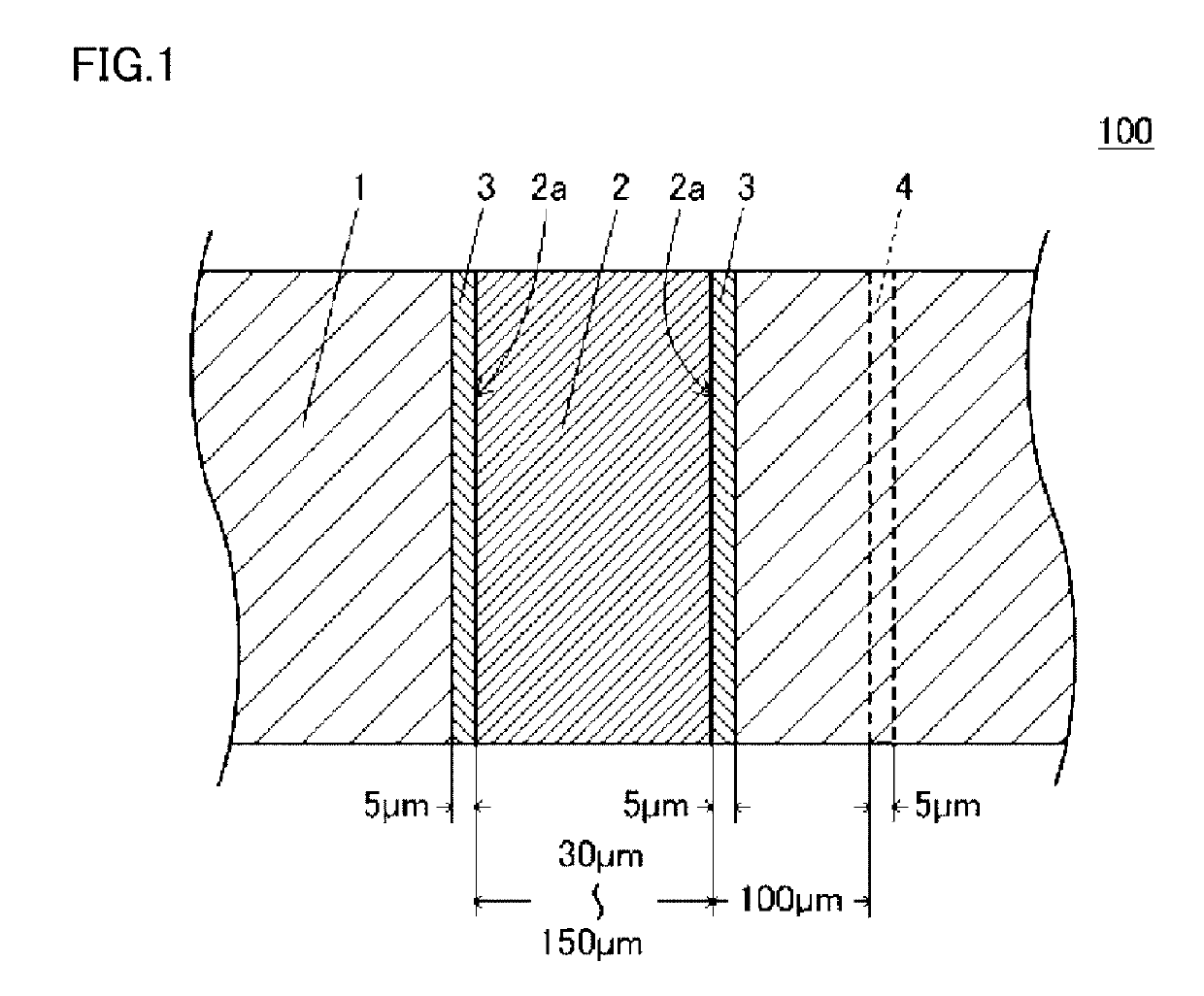
[0084]A ceramic wiring board 100 according to an embodiment of the present invention is described below with reference to FIG. 1. The ceramic wiring board 100 is used as a wiring board on which active components such as an IC chip and passive components such as a capacitor are mounted and wired to one another to form a module.

[0085]FIG. 1 is a diagram schematically illustrating a cross section of the ceramic wiring board 100. The ceramic wiring board 100 includes a ceramic insulator 1 and a via-conductor 2. In this embodiment, the ceramic insulator 1 includes, as described below, SiO2, Al2O3, celsian (BaAl2Si2O8), and fresnoite (Ba2TiSi2O8) that serve as crystalline constituents. The ceramic insulator 1 also includes a glass constituent including oxides of Si, Ba, Mn, Al, Ti, Zr, and Mg which serve as ...


PUM

PropertyMeasurementUnit
thicknessaaaaaaaaaa
diameteraaaaaaaaaa
specific surface areaaaaaaaaaaa

Abstract

A ceramic wiring board that includes a ceramic insulator and a via-conductor. The ceramic insulator includes a crystalline constituent and an amorphous constituent. The via-conductor includes a metal and an oxide. The crystalline constituent and the oxide include at least one metal element in common. A tubular region having a thickness of 5 μm adjoins and surrounds the via-conductor and has a higher concentration of the metal element than the ceramic insulator.

Description

CROSS REFERENCE TO RELATED APPLICATIONS[0001]The present application is a continuation of International application No. PCT / JP2016 / 062132, filed Apr. 15, 2016, which claims priority to Japanese Patent Application No. 2015-085304, filed Apr. 17, 2015, the entire contents of each of which are incorporated herein by reference.FIELD OF THE INVENTION[0002]The present invention relates to a ceramic wiring board and a method for producing the ceramic wiring board and specifically to a ceramic wiring board that includes a ceramic insulator including crystalline constituents and an amorphous constituent, that is, a “glass-ceramic” insulator.BACKGROUND OF THE INVENTION[0003]Ceramic wiring boards include a ceramic insulator, via-conductors arranged to be orthogonal to the principal plane of the ceramic insulator, pattern conductors arranged to be parallel to the principal plane of the ceramic insulator, and mounting electrodes disposed on the principal plane of the insulator. The ceramic wirin...

Claims


Application Information

Patent Timeline
Patent Type & Authority Patents(United States)
IPC IPC(8): H05K1/03H05K3/12H05K3/40H05K1/09H05K1/11H05K3/00H05K3/22H05K3/46
CPCH05K1/0306H05K1/09H05K1/115H05K3/0044H05K3/1291H05K3/22H05K3/4038H05K3/4061H05K3/4647H05K3/4629H05K2201/0175H05K2201/098H05K2201/09563H05K2201/09809H05K2203/1126
Inventor SUMI, TAKAHIROOKA, TAKAHIROYAMAGAMI, YOSHITAKE
Owner MURATA MFG CO LTD
Why Eureka
Try Eureka