
Display device and method of manufacturing the same

a technology of display device and manufacturing method, which is applied in the direction of identification means, instruments, and details of portable computers, etc., can solve the problems of low design freedom of hmd, large thickness of eyepiece, and large thickness of entire hmd

Active Publication Date: 2022-06-07
SAMSUNG DISPLAY CO LTD
View PDF20 Cites 0 Cited by
  • Summary
  • Abstract
  • Description
  • Claims
  • Application Information

AI Technical Summary

Benefits of technology

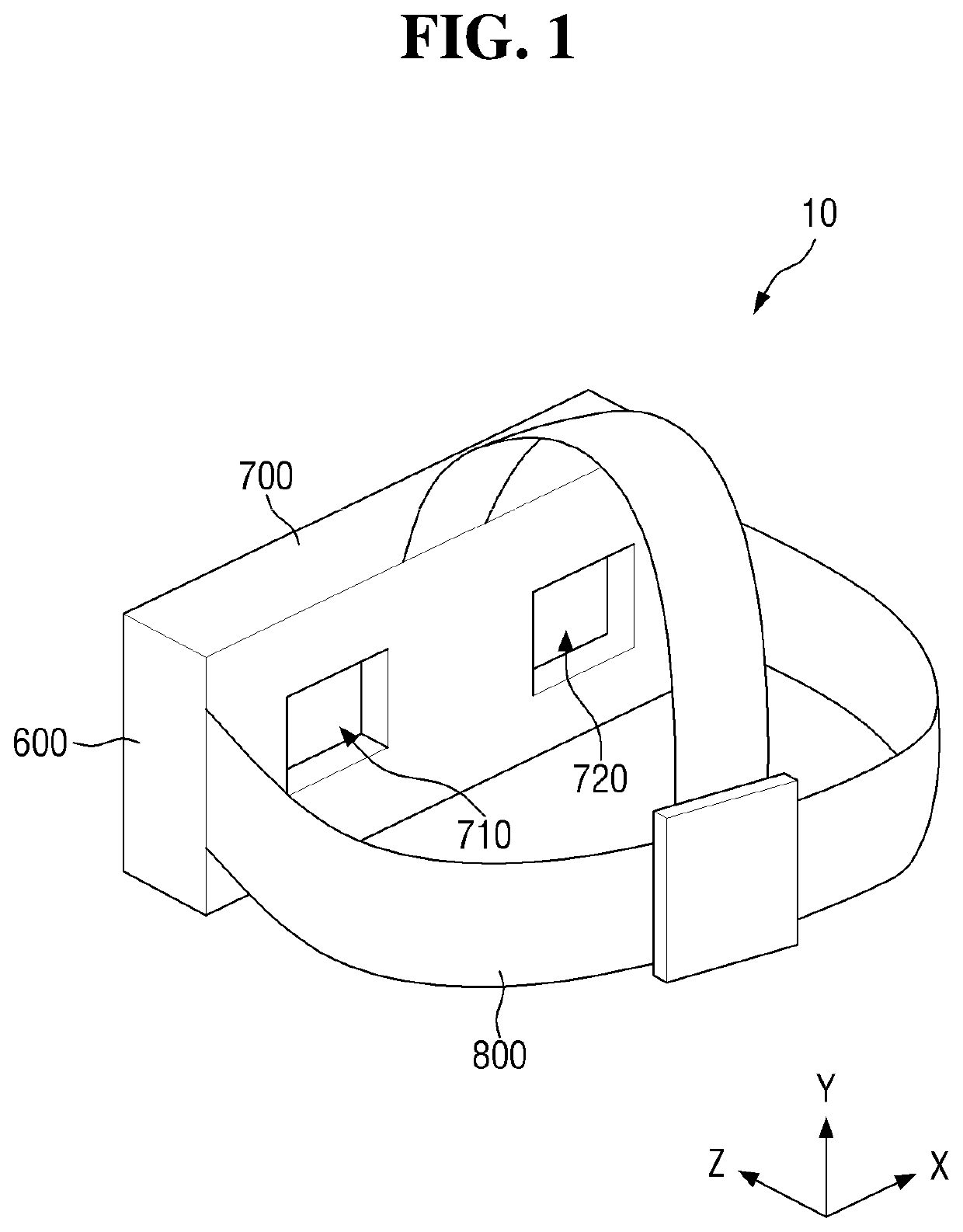
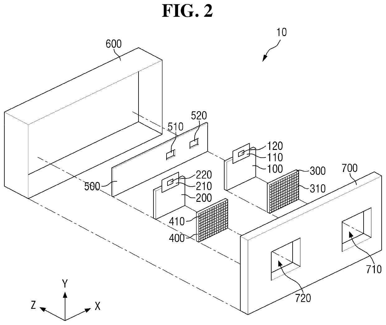
[0006]One or more aspects of example embodiments of the present disclosure provide a display device applicable to a head mounted display (HMD) that can be slimmed down by eliminating an eyepiece.
[0007]One or more aspects of example embodiments of the present disclosure also provide a method of manufacturing a display device applicable to an HMD that can be slimmed down by eliminating an eyepiece.
[0032]According to the aforementioned and other example embodiments of the present disclosure, since a lens array including lenses is on a display panel, a series of view images can be provided to a location where the eyes of a user are placed. Thus, an enlarged virtual image from an image actually displayed by a display panel can be provided to the user without the aid of an eyepiece. Accordingly, an eyepiece can be eliminated, and as a result, the thickness of a display device can be considerably reduced.
[0035]Also, since view images displayed by sub-pixels are enlarged and displayed in view images via lenses, a screen door effect in which a black matrix is enlarged and viewed as a lattice can be prevented.
[0036]Also, since the lens array including the lenses is formed directly on the display panel, alignment error between the lenses and sub-pixels can be reduced.

Problems solved by technology

However, the eyepiece is generally thick because it consists of convex lenses having a large volume.
Accordingly, the entire HMD becomes thick, and the design freedom of the HMD is low.

Method used


Image

  • Display device and method of manufacturing the same
  • Display device and method of manufacturing the same
  • Display device and method of manufacturing the same

Examples


Embodiment Construction

[0059]The present disclosure will now be described more fully hereinafter with reference to the accompanying drawings, in which preferred embodiments of the disclosure are shown. This disclosure may, however, be embodied in different forms and should not be construed as limited to the embodiments set forth herein. Rather, these embodiments are provided so that this disclosure will be thorough and complete, and will fully convey the scope of the disclosure to those skilled in the art. The same reference numbers indicate the same components throughout the specification. In the attached figures, the thickness of layers and regions is exaggerated for clarity.

[0060]It will also be understood that when a layer is referred to as being “on” another layer or substrate, it can be directly on the other layer or substrate, or intervening layers may also be present. In contrast, when an element is referred to as being “directly on” another element, there are no intervening elements present.

[0061...


PUM

PropertyMeasurementUnit
distanceaaaaaaaaaa
refractive indexaaaaaaaaaa
sizeaaaaaaaaaa

Abstract

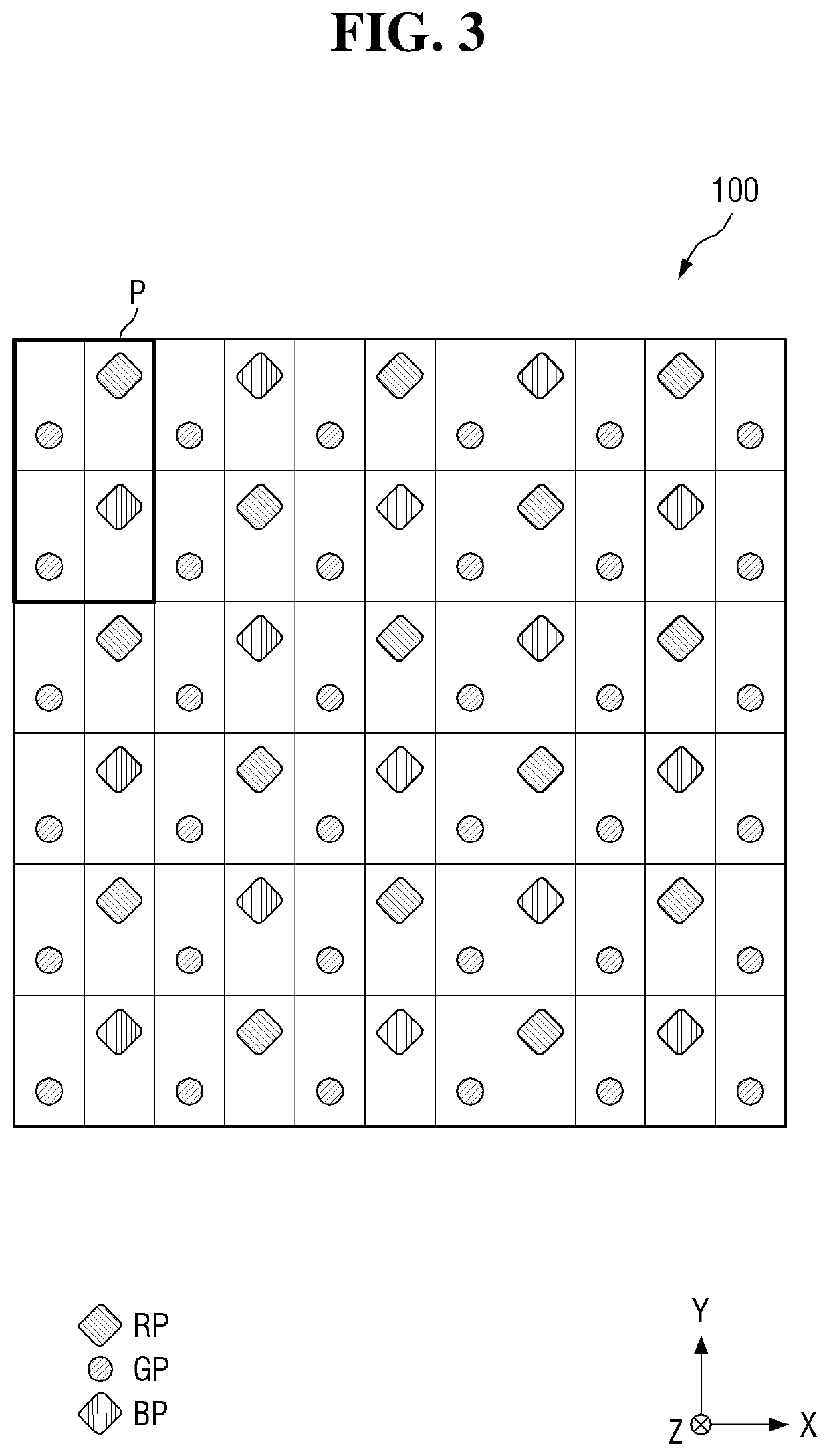
A display device and a method of manufacturing the same are provided. The display device includes a display panel including a series of pixels, each pixel including N sub-pixels, where N is an integer of 2 or greater; and a lens array on a surface of the display panel, the lens array including a series of lenses, wherein each of the lenses overlaps with M sub-pixels, where M is an integer greater than N.

Description

CROSS-REFERENCE TO RELATED APPLICATION[0001]This application claims priority to and the benefit of Korean Patent Application No. 10-2018-0114435, filed on Sep. 21, 2018 in the Korean Intellectual Property Office, the entire content of which is incorporated herein by reference.BACKGROUND1. Field[0002]One or more aspects of example embodiments of the present disclosure relate to a display device and a method of manufacturing the same.2. Description of the Related Art[0003]A head mounted display (HMD) is a display device that can be worn on the head of a user or as part of a helmet or glasses and can form a focal point at a distance close to the eyes of the user. The HMD can be utilized for virtual reality (VR) or augmented reality (AR).[0004]The HMD may include an eyepiece on which the eyes of the user can be placed and a display module which displays an image. In the HMD, the eyepiece is disposed between the eyes of the user, and the display module, which displays an image, is dispos...

Claims


Application Information

Patent Timeline
Patent Type & Authority Patents(United States)
IPC IPC(8): H01L27/15G02B3/00G03F7/20H01L27/32H01L51/52G06F1/16
CPCG02B3/0037G02B3/0012G03F7/70058H01L27/322H01L51/5275G06F1/163G02B27/0101G09F9/33G02B27/0172G02B3/0006H10K50/858H10K59/38
Inventor HA, JU HWAKWON, JAE JOONGKIM, BEOM SHIKCHO, JOO WOANHUH, SU JUNG
Owner SAMSUNG DISPLAY CO LTD
Learn More