Check patentability & draft patents in minutes with Patsnap Eureka AI!

Array substrate and liquid crystal display panel

a liquid crystal display panel and array substrate technology, applied in the field of display technology, can solve the problems of poor film surface or thickness precision of polyimide film, undesirable display brightness, etc., and achieve the effect of reducing the length of one end

Active Publication Date: 2022-06-14
WUHAN CHINA STAR OPTOELECTRONICS TECH CO LTD
View PDF10 Cites 0 Cited by
  • Summary
  • Abstract
  • Description
  • Claims
  • Application Information

AI Technical Summary

Benefits of technology

This approach reduces the occurrence of Mura phenomena by ensuring smooth fluid flow and preventing film thickness variations, resulting in uniform liquid crystal alignment and improved display quality.

Problems solved by technology

In a liquid crystal display (LCD) panel industry, uneven display brightness (Mura) is an undesirable phenomenon that affects yield of panels, such as peripheral Mura, horizontal Mura, and diagonal Mura.
On the one hand, a difference in manufacturing process will cause a film surface or thickness precision of the polyimide film to be poor, wherein temperature, time, dispensed amounts, and print speed in the manufacturing process will all cause the film surface or thickness precision of the polyimide film to be poor.
On the other hand, panel design can also cause poor film surface or thickness precision of the polyimide film.
As a result, an area thicker than other normal areas will be formed at a boundary position between the display area and a non-display area, which will cause abnormal liquid crystal deflection, and Mura phenomenon will occur during lighting inspection.
Therefore, how to solve the technical problem of an abnormal coating of the polyimide film due to a current PLN via-hole, which further leads to a Mura phenomenon in LCD panels, is a problem that panel manufacturers all over the world have to overcome.

Method used


Image

  • Array substrate and liquid crystal display panel
  • Array substrate and liquid crystal display panel
  • Array substrate and liquid crystal display panel

Examples


Embodiment Construction

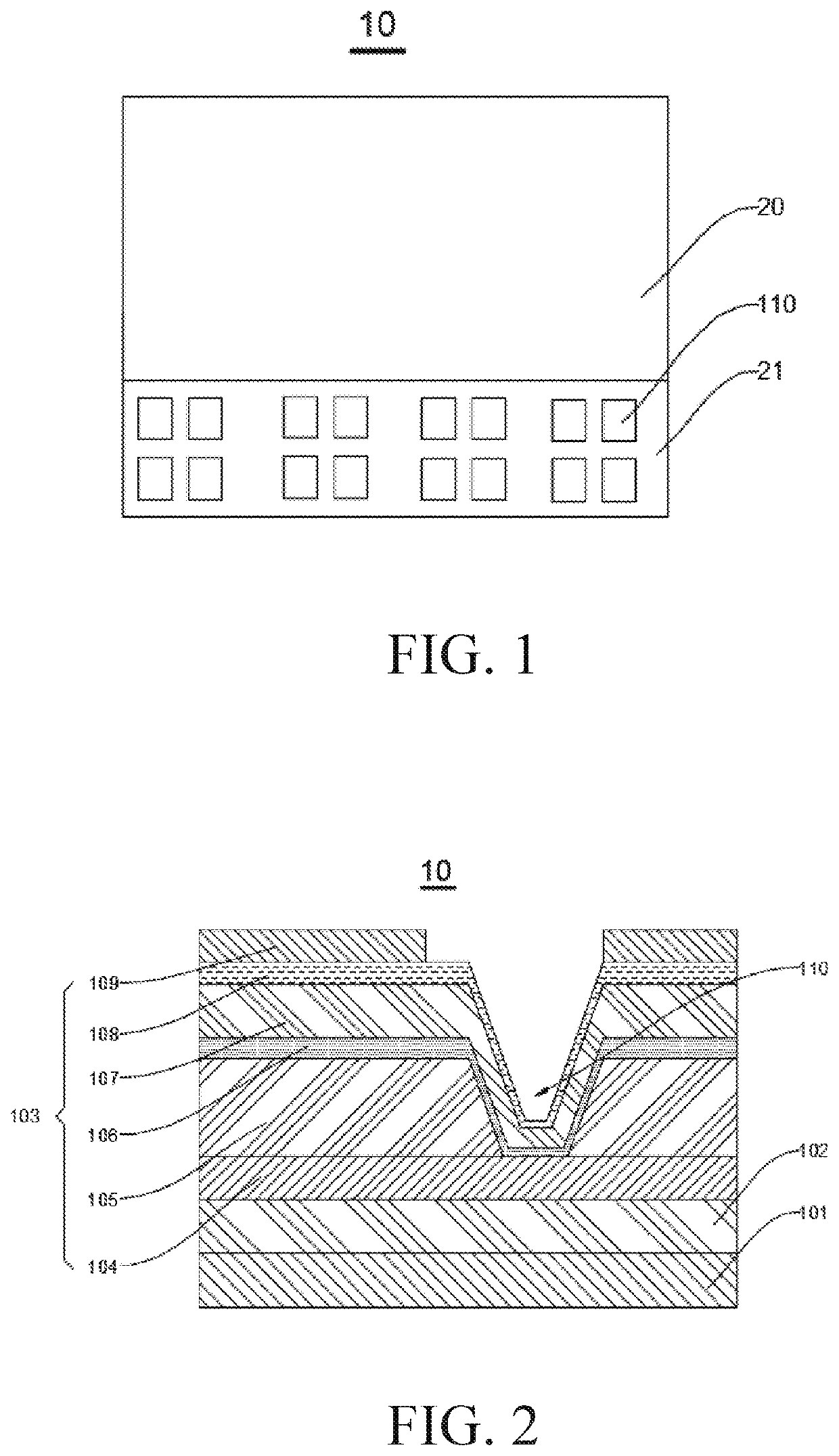
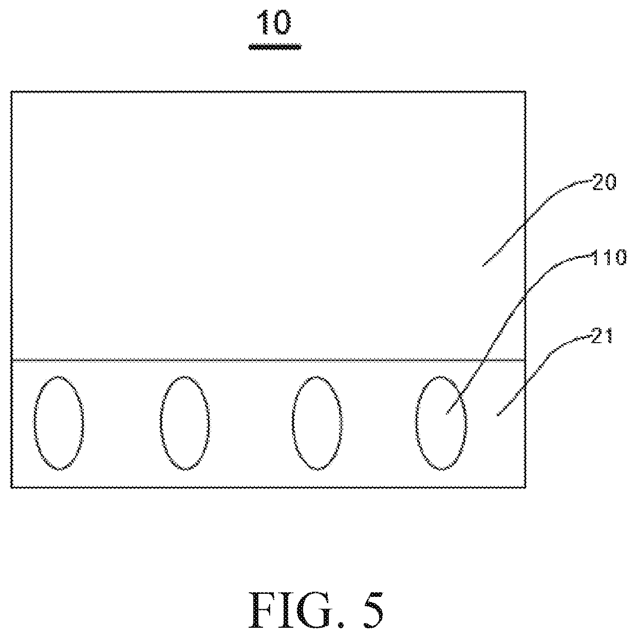
[0034]The technical solutions in the embodiments of the present application will be clearly and completely described below with reference to the drawings in the embodiments of the present application. Obviously, the described embodiments are only a part of the embodiments of the present application, rather than all the embodiments. Based on the embodiments in this application, all other embodiments obtained by those skilled in the art without doing creative work are within the protection scope of this application.

[0035]Following disclosure provides various embodiments or examples for realizing different structures of the present application. To simplify the disclosure of the present application, components and settings of specific examples are described below. Certainly, they are only examples and are not intended to limit the application. Moreover, the present application may repeat reference numerals and / or reference letters in different examples, and this repetition is for the pu...


PUM

PropertyMeasurementUnit
lengthaaaaaaaaaa
distanceaaaaaaaaaa
widthaaaaaaaaaa

Abstract

An array substrate and a liquid crystal display panel are provided, wherein the array substrate includes a display area and a non-display area, and a length of one end of via-holes close to the display area is not greater than 12.5 microns. By reducing a length of one end of the via-holes positioned at a boundary position between the display area and the non-display area close to the display area, a flow of polyimide fluid is guided and enables an edge of a polyimide film to cover an area where the via-holes are located.

Description

FIELD OF INVENTION[0001]The application relates to a field of display technology, in particular to an array substrate and a liquid crystal display panel.BACKGROUND OF INVENTION[0002]In a liquid crystal display (LCD) panel industry, uneven display brightness (Mura) is an undesirable phenomenon that affects yield of panels, such as peripheral Mura, horizontal Mura, and diagonal Mura. Wherein, Mura caused by precision of a polyimide film and a film surface accounts for a majority.[0003]Reasons for poor polyimide film are various. On the one hand, a difference in manufacturing process will cause a film surface or thickness precision of the polyimide film to be poor, wherein temperature, time, dispensed amounts, and print speed in the manufacturing process will all cause the film surface or thickness precision of the polyimide film to be poor. On the other hand, panel design can also cause poor film surface or thickness precision of the polyimide film.[0004]In current design, when polyim...

Claims


Application Information

Patent Timeline
Patent Type & Authority Patents(United States)
IPC IPC(8): G02F1/1345G02F1/1343G02F1/1362
CPCG02F1/13452G02F1/13454G02F1/13456G02F1/13458G02F1/134363G02F1/1362G02F1/133723G02F1/133388G02F2201/501G02F1/1303
Inventor HUANG, JIANLONG
Owner WUHAN CHINA STAR OPTOELECTRONICS TECH CO LTD
Features
  • R&D
  • Intellectual Property
  • Life Sciences
  • Materials
  • Tech Scout
  • Unparalleled Data Quality
  • Higher Quality Content
  • 60% Fewer Hallucinations
Learn More