Package integration for laterally mounted IC dies with dissimilar solder interconnects

a technology of laterally mounted ic dies and solder interconnects, which is applied in the direction of semiconductor devices, semiconductor/solid-state device details, electrical apparatus, etc., can solve the problems of failure of the solder joint and the ic device itself, damage to the routings within the redistribution layer, and even more problems such as cracking. to achieve the effect of enhancing the reliability of the redistribution layer

Active Publication Date: 2022-06-28
XILINX INC
View PDF15 Cites 2 Cited by
  • Summary
  • Abstract
  • Description
  • Claims
  • Application Information

AI Technical Summary

Benefits of technology

[0005]A chip package assembly and method of fabricating the same are described herein. The chip package assembly generally includes at least one integrated circuit (IC) die that

Problems solved by technology

Notably, the reliability of the integrated circuit interconnects, e.g., solder joints, is one of the most critical issues for successful application of such mounting and connection methods.
However, redistribution layers formed using known methods are prone to cracking, which may lead to failure of the solder joint and IC device itself.
The propensity for cracking is even more problematic in packages having a first die with a solder joint that extends further fro

Method used


Image

  • Package integration for laterally mounted IC dies with dissimilar solder interconnects
  • Package integration for laterally mounted IC dies with dissimilar solder interconnects
  • Package integration for laterally mounted IC dies with dissimilar solder interconnects

Examples


Embodiment Construction

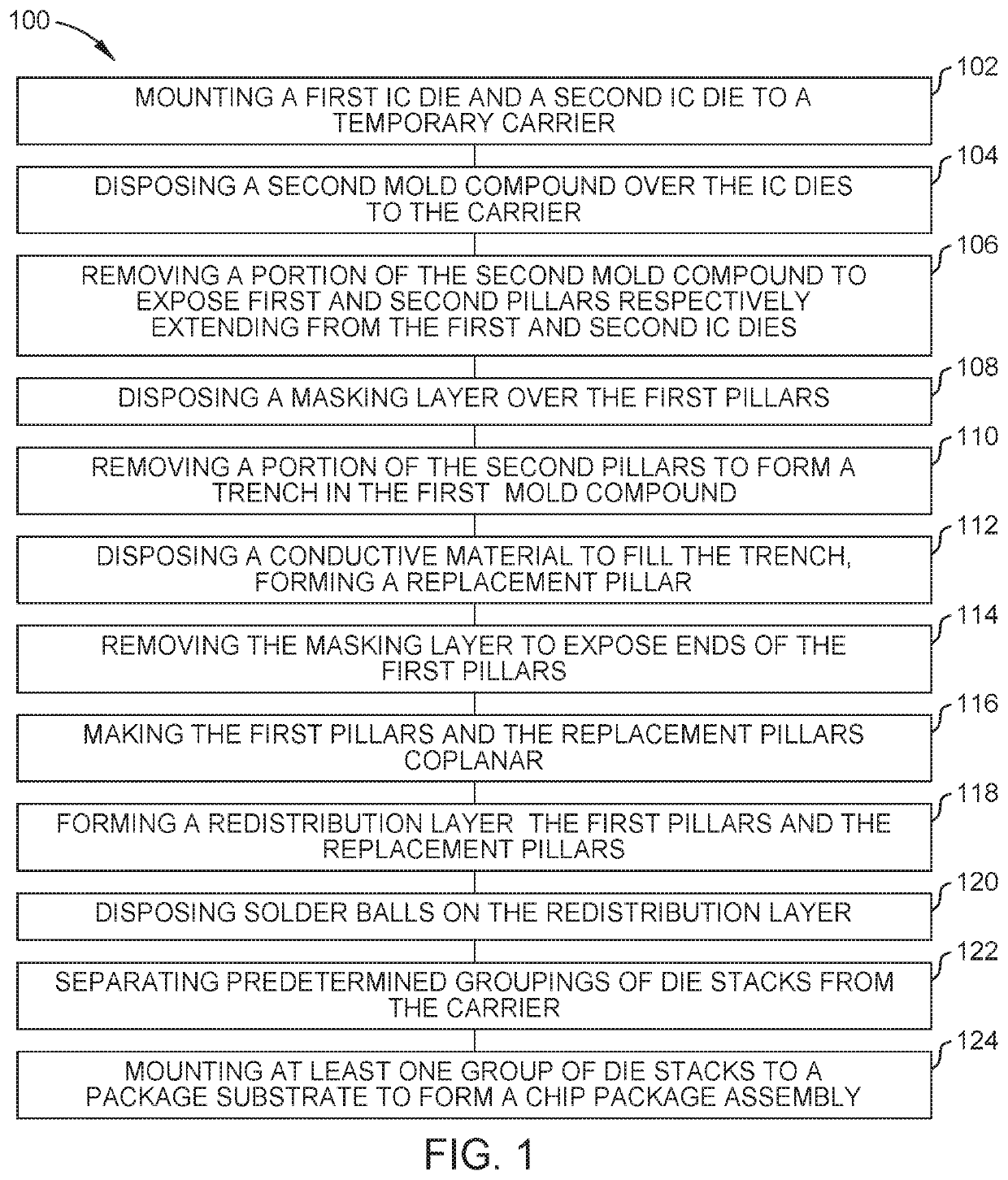
[0013]Examples described herein generally provide chip package assemblies having at least two dies mounted laterally to a substrate and methods of fabricating the same. The chip package assemblies described herein generally include at least one integrated circuit (IC) die having the original solder interconnects at least partially replaced to enhance the reliability of a redistribution layer disposed between the IC die and the package substrate in chip packages having a neighboring IC die with solder interconnects having different initial heights. Consequently, the amount of material removal required to make pillars of the neighboring IC dies coplanar is significantly reduced compared to conventional design, which substantially prevents cracking and damage to the redistribution layer disposed between the IC die and the package substrate. As a result, the neighboring IC dies are connected to the substrate with a more robust and reliable solder joint, and accordingly, form a more robu...


PUM


Abstract

A chip package assembly and method of fabricating the same are described herein. The chip package assembly generally includes at least one integrated circuit (IC) die that has had the original solder interconnects at least partially replaced to enhance the reliability of a redistribution layer disposed between the IC die and the substrate. In the resulting chip package assembly, at least one IC die includes first and second pillars extending from exposed contact pads through a first mold compound. The second pillars are fabricated from a material that has a composition different than that of the first pillars. A redistribution layer is formed on the first and second pillars. The solder interconnects mechanically couple the redistribution layer to landing pads of a substrate. The solder interconnects also electrically couple circuitry of the substrate to the circuitry of the IC die through the redistribution layer and first and second pillars.

Description

TECHNICAL FIELD[0001]Embodiments of the present disclosure generally relate to chip packages and electronic devices having the same. In particular, to chip packages having at laterally spaced integrated circuit (IC) dies having solder interconnects at initially dissimilar heights.BACKGROUND ART[0002]Electronic devices, such as tablets, computers, server, in-door telecom, out-door telecom, industrial computers, high performance computing data centers, copiers, digital cameras, smart phones, control systems and automated teller machines, among others, often employ electronic components which leverage chip packages for increased functionality and higher component density. Conventional chip packages include one or more stacked components such as integrated circuit (IC) dies, through-silicon-via (TSV) interposer, and a package substrate, with the chip package itself stacked on a printed circuit board (PCB). The IC dies may include memory, logic, MEMS, RF or other IC device.[0003]In flip-...

Claims


Application Information

Patent Timeline
IPC IPC(8): H01L25/18H01L25/00H01L23/00
CPCH01L25/18H01L24/19H01L24/20H01L25/50H01L2924/1431H01L2924/1434H01L2924/3512H01L25/0652H01L2225/06513H01L2225/06517H01L25/105H01L2225/06527H01L2224/16145H01L2224/16225
Inventor GANDHI, JASPREET SINGHRAMALINGAM, SURESH
Owner XILINX INC
Why Eureka
Try Eureka