Dimming panel, dimming unit, and liquid crystal display device

a technology of dimming unit and dimming panel, which is applied in the direction of static indicating device, non-linear optics, instruments, etc., can solve the problems of large brightness difference and significant size of local dimming illumination areas

Active Publication Date: 2022-08-09
SHARP KK
View PDF5 Cites 2 Cited by
  • Summary
  • Abstract
  • Description
  • Claims
  • Application Information

AI Technical Summary

Benefits of technology

[0008]The present inventors studied another method for increasing the contrast ratio of a liquid crystal display device, including disposing a dimming panel between an image-providing liquid crystal panel and a backlight. The study demonstrated that provision of a dimming panel can control the amount of light emitted from the backlight (hereinafter, also referred to as backlight illumination) and transmitted through each dimming unit constituting the dimming panel, which can reduce the halo phenomenon while increasing the contrast ratio of the liquid crystal display device.
[0011]A study made in WO 2008 / 053724 is that in order to smooth the luminance difference between dimming units, the boundary between adjacent dimming units constituting the dimming panel is made irregular (zigzag) and thereby the luminance distribution is smoothly changed. According to studies by the present inventors, however, in a horizontally aligned dimming panel, making a boundary between dimming units zigzag as disclosed in WO 2008 / 053724 fails to smoothly change the luminance distribution and rather causes zigzag dark lines. When a dimming panel having an unsmooth luminance distribution provides images of different scales in adjacent dimming units, the luminance difference between the dimming units unfortunately becomes remarkable. Dimming units constituting a dimming panel are larger than the pixels constituting the image-providing liquid crystal panel, and thus the outlines thereof are unintendedly recognized in some cases when the dimming panel is stacked on the image-providing liquid crystal panel. Studies by the present inventors further revealed that in display with a horizontally aligned dimming panel, liquid crystal molecules possibly have an alignment defect at the boundaries between dimming units and thereby cause dark lines. Appearance of such dark lines emphasizes the boundaries between dimming units, and thereby not only reduces the display quality of the dimming panel but also reduces the transmittance of the dimming panel.
[0013]The present invention is made under the current situation in the art and aims to provide a dimming panel that has a high transmittance and a smooth change in luminance distribution, and a liquid crystal display device including the dimming panel.
[0028]The present invention can provide a dimming panel that has a high transmittance and a smooth change in luminance distribution, and a dimming unit and a liquid crystal display device including the dimming panel.

Problems solved by technology

Unfortunately, the illuminating areas for local dimming have a significantly greater size than the pixel size of the image-providing liquid crystal panel.
This may result in a halo phenomenon that causes a portion which should be displayed dark to look brightly at a boundary between images with a large difference in brightness.

Method used


Image

  • Dimming panel, dimming unit, and liquid crystal display device
  • Dimming panel, dimming unit, and liquid crystal display device
  • Dimming panel, dimming unit, and liquid crystal display device

Examples


example 1

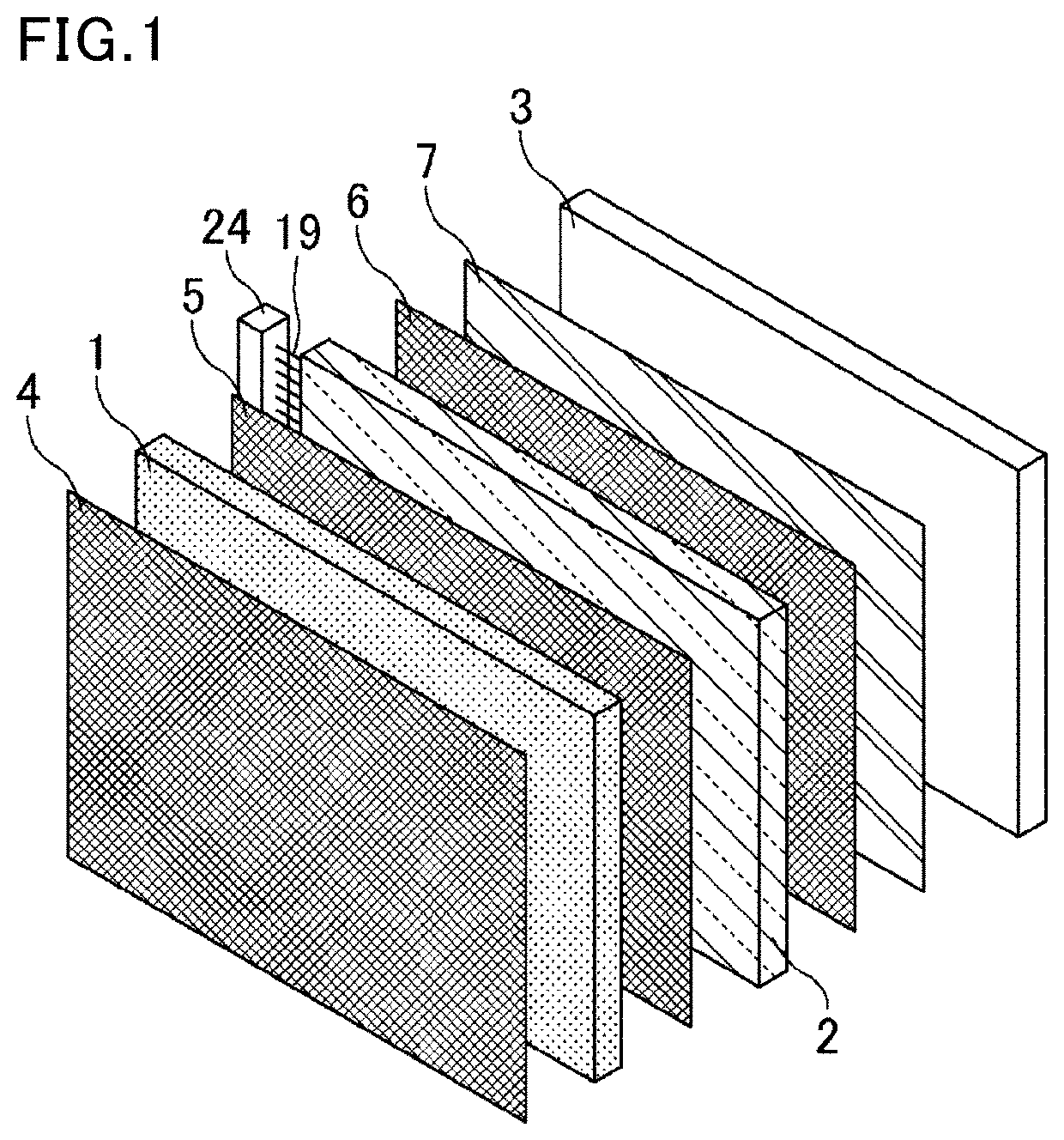
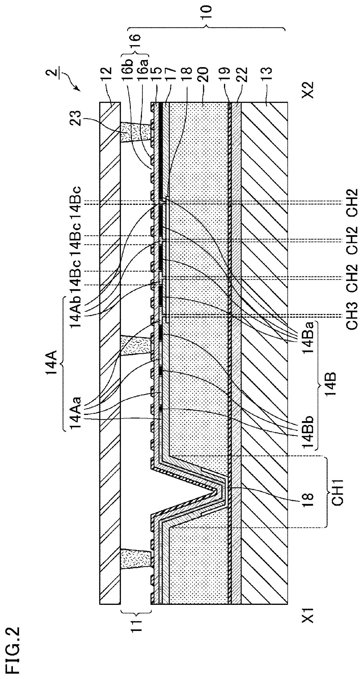
[0114]FIG. 1 is an exploded perspective view of a liquid crystal display device of Example 1. As shown in FIG. 1, the liquid crystal display device of Example 1 includes an image-providing liquid crystal panel 1, a backlight 3, and a dimming panel 2 between the image-providing liquid crystal panel 1 and the backlight 3. A pair of polarizers may be disposed on the surfaces of the image-providing liquid crystal panel 1 and on the surfaces of the dimming panel 2. As shown in FIG. 1, a first polarizer 4, the image-providing liquid crystal panel 1, a second polarizer 5, the dimming panel 2, and a third polarizer 6 may be disposed in this order. The image-providing liquid crystal panel 1 and the dimming panel 2 may share the second polarizer 5 disposed therebetween. The first polarizer 4 and the second polarizer 5 are arranged with their absorption axes being perpendicular to each other. The second polarizer 5 and the third polarizer 6 are arranged with their absorption axes being perpend...

example 2

[0136]Hereinafter, a liquid crystal display device of Example 2 is described with reference to FIG. 15 to FIG. 18. The liquid crystal display device of Example 2 has the same structure as that of Example 1 except for the structure of the first electrodes used in the dimming panel. The description for the structures similar to the liquid crystal display device of Example 1 is omitted here. FIG. 15 is a schematic plan view showing one of first electrodes used in a dimming panel of Example 2. FIG. 16 is a plan view of the first electrodes arranged with reference to the pixels of the image-providing liquid crystal panel. FIG. 18 is a schematic plan view of the dimming panel in Example 2, showing an example of a method for driving the first electrodes. FIG. 17 is a schematic plan view showing an arrangement example of first electrodes shown in FIG. 15. In FIG. 15 and FIG. 17, the portions surrounded by two-dot chain lines are positioning areas for locating the first electrodes. In FIG. 1...

example 3

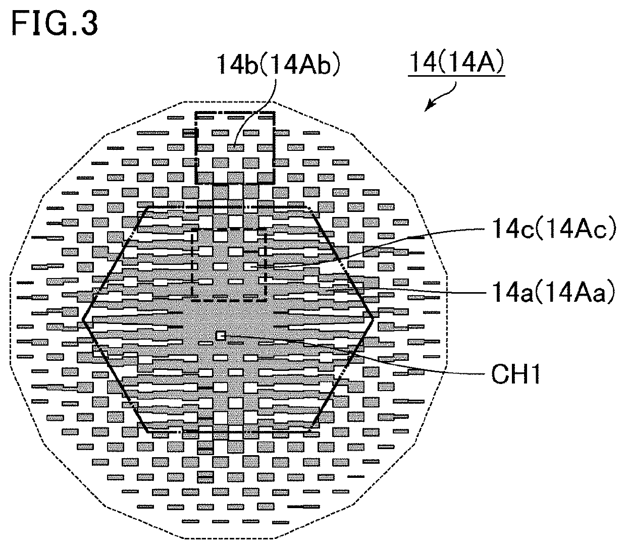
[0143]Hereinafter, a liquid crystal display device of Example 3 is described with reference to FIG. 19 to FIG. 25 and FIG. 26A to FIG. 26C. The liquid crystal display device of Example 3 has the same structure as that of Example 1 except for the structure of the first electrodes used in the dimming panel. The description for the structures similar to the liquid crystal display device of Example 1 is omitted here. FIG. 19 is a schematic plan view showing one of first electrodes used in a dimming panel of Example 3. FIG. 20 is a schematic plan view showing an arrangement example of first electrodes shown in FIG. 19. In FIG. 19 and FIG. 20, the portions surrounded by two-dot chain lines are base electrodes.

[0144]As shown in FIG. 19, the outer peripheral shape of the positioning areas for locating the first electrodes in Example 3 is a quadrangle (square). Each base electrode 214a is provided with multiple apertures 214c (214Ac). Multiple island electrodes 214b (214Ab) surround the base...


PUM

PropertyMeasurementUnit
angleaaaaaaaaaa
angleaaaaaaaaaa
gap widthaaaaaaaaaa

Abstract

The present invention relates to a dimming panel sequentially including a first substrate, a liquid crystal layer, and a second substrate, the first substrate sequentially including an insulating substrate, multiple first electrodes, a first insulating layer, and a second electrode including parallel linear electrodes, each of the first electrodes including a base electrode and multiple island electrodes, the base electrode being provided with multiple apertures, the island electrodes being electrically connected to the base electrode, surrounding the base electrode in a plan view, and being arranged with intervals, at least one of the island electrodes of a selected electrode of the first electrodes being disposed in at least one position selected from the group consisting of a position inside at least one of the apertures of a next electrode and a position between adjacent two of the island electrodes of the next electrode.

Description

CROSS-REFERENCE TO RELATED APPLICATIONS[0001]The present application claims priority under 35 U.S.C. § 119 to U.S. provisional Patent Application No. 63 / 002,386 filed on Mar. 31, 2020, the contents of which are incorporated herein by reference in their entirety.BACKGROUND OF THE INVENTIONField of the Invention[0002]The present invention relates to dimming panels, dimming units including the dimming panel, and liquid crystal display devices including the dimming panel.Description of Related Art[0003]Dimming panels are panels that can control the transmittance of light in response to the voltage applied to the panel. For example, a dimming panel can be used as an optical member that is placed between an image-providing liquid crystal panel and a backlight and controls the amount of backlight illumination transmitted, or as a member that controls the amount of external light transmitted into a building, a vehicle, or the like. One of dimming methods using such a dimming panel includes ...

Claims


Application Information

Patent Timeline
Patent Type & Authority Patents(United States)
IPC IPC(8): G09G3/36G09G3/34G02F1/1335G02F1/1347G02F1/1343
CPCG09G3/3413G02F1/13471G02F1/133601G02F1/133612G02F1/134363G02F1/134372G09G3/36G02F2201/122G09G2300/0426G09G2300/0452G02F1/134309G02F1/1347G02F1/134336
Inventor SHIMOSHIKIRYOH, FUMIKAZUYOSHIDA, TAKEHISAYAMADA, SHIGEYUKI
Owner SHARP KK
Why Eureka
Try Eureka