Low-cost and low-voltage anti-fuse array

a low-cost, anti-fuse technology, applied in the direction of semiconductor devices, semiconductor/solid-state device details, instruments, etc., can solve the problems of increasing the cost, requiring the application of voltage large enough to puncture through the gate dielectric layer, and requiring leakage current to flow to the anti-fuse memory cell through the unselected bit-line bl, so as to reduce the cell area, reduce costs, and stabilize the source structure

Active Publication Date: 2022-11-15
YIELD MICROELECTRONICS CORP
View PDF2 Cites 0 Cited by
  • Summary
  • Abstract
  • Description
  • Claims
  • Application Information

AI Technical Summary

Benefits of technology

[0005]Aiming at solving the above problem, the main objective of the present invention is to provide a low-cost and low-voltage anti-fuse array, which utilizes the configuration of common source contacts to reduce the cell area, stabilize the source structure and reduce costs. In addition, the present invention may further minimize the types of control voltages to avoid the occurrence of leakage current.
[0006]To achieve the above objective, the present invention provides a low-cost and low-voltage anti-fuse array, which comprises a plurality of parallel bit-lines, a plurality of parallel word-lines, a plurality of parallel selection-lines and a plurality of sub-memory arrays. The parallel bit-lines comprises adjacent first bit-line and second bit-line; the parallel word-lines are perpendicular to the bit-lines and comprise a first word-line, a second word-line, a third word-line and a fourth word-line; the parallel selection-lines are parallel to the word-lines and comprise a first selection-line; and each of the sub-memory arrays comprises a first anti-fuse memory cell, a second anti-fuse memory cell, a third anti-fuse memory cell and a fourth anti-fuse memory cell. The first anti-fuse memory cell is connected to the first word-line, the first selection-line and the first bit-line. The second anti-fuse memory cell is connected to the second word-line, the first selection-line and the second bit-line, wherein the first anti-fuse memory cell and the second anti-fuse memory cell are adjacent to each other along the horizontal direction. The third anti-fuse memory cell is connected to the third word-line, the first selection-line and the first bit-line, wherein the third anti-fuse memory cell and the first anti-fuse memory cell are adjacent to each other along the vertical direction. The fourth anti-fuse memory cell is connected to the fourth word-line, the selection-line and the second bit-line, wherein the fourth anti-fuse memory cell is located at an intersection of the horizontal direction of the third anti-fuse memory cell and the vertical direction of the second anti-fuse memory cell, and the first, second, third and fourth anti-fuse memory cell are located between the first bit-line and the second bit-line. Each of the first, second, third and fourth anti-fuse memory cell has an anti-fuse transistor, and only one of the corners of a first gate dielectric layer of the anti-fuse transistor overlaps an anti-fuse gate.
[0007]The first, second, third and fourth anti-fuse memory cells all comprise an anti-fuse transistor. The first gate dielectric layer of the anti-fuse transistor only has one corner that overlaps the anti-fuse gate. In one embodiment, each of the four corners of the anti-fuse gate of the anti-fuse transistor overlaps with a corner of a different first gate dielectric layer, making the anti-fuse gate shared by four first gate dielectric layers. Specifically, each intersection of the anti-fuse gate and each first gate dielectric layer has a protruding corner. During operation, the charge density at the protruding corner is higher and therefore can reduce the puncturing voltage and thereby lower the current requirement of programming the anti-fuse memory cell, and meanwhile also reduce the area of components.

Problems solved by technology

Since the anti-fuse transistor forms a permanent conductive path substrated on the rupture of the gate dielectric layer, one limitation is that a voltage large enough to puncture through the gate dielectric layer must be applied.
However, when this anti-fuse array selects an anti-fuse memory cell 1 for writing, other unselected anti-fuse memory cells 1 are susceptible to the selection bias voltage, which may cause leakage current to flow to the anti-fuse memory cell through the unselected bit-line BL1.
In this way, the source structure is not stable enough, thereby raising the cost.

Method used


Image

  • Low-cost and low-voltage anti-fuse array
  • Low-cost and low-voltage anti-fuse array
  • Low-cost and low-voltage anti-fuse array

Examples


Embodiment Construction

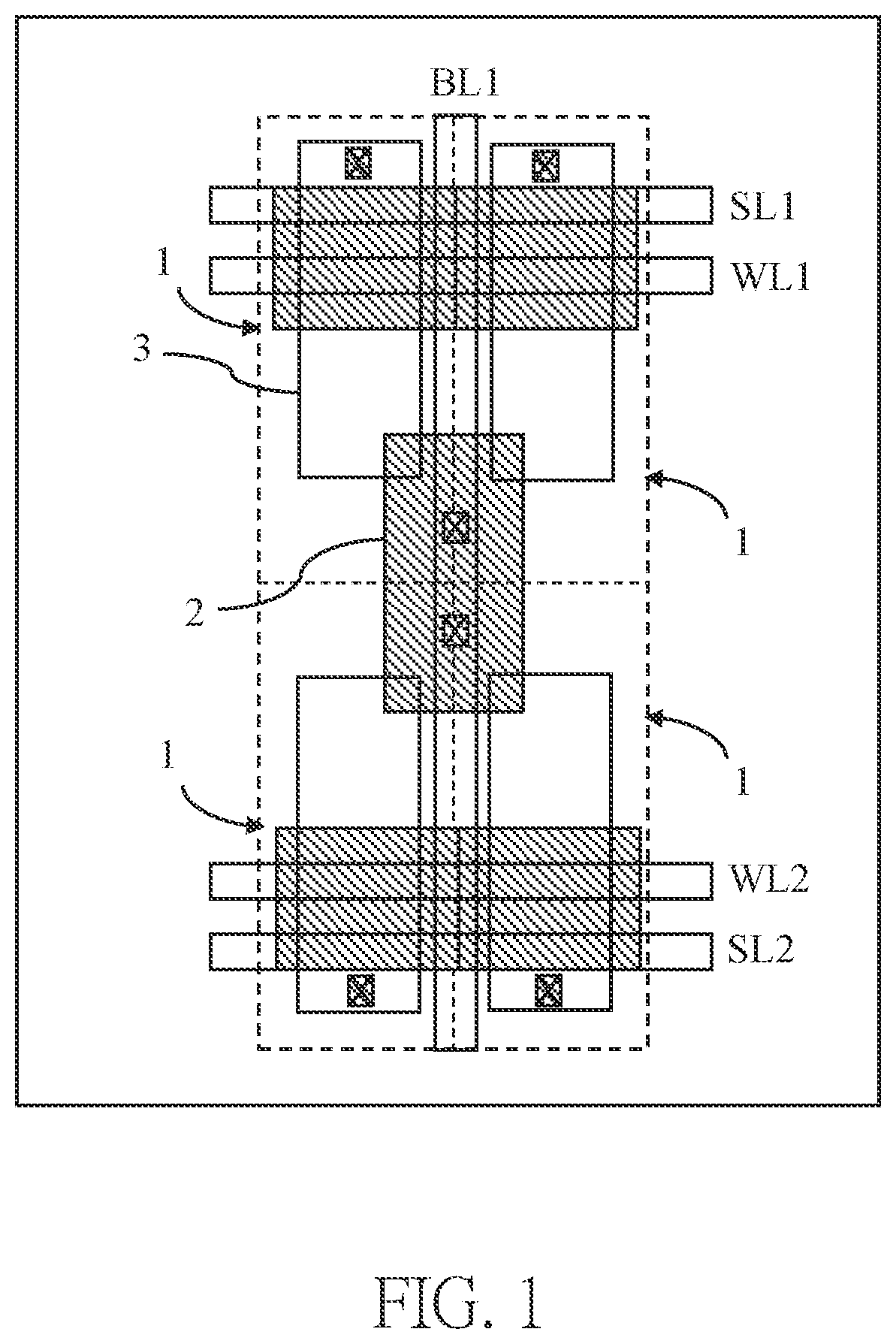
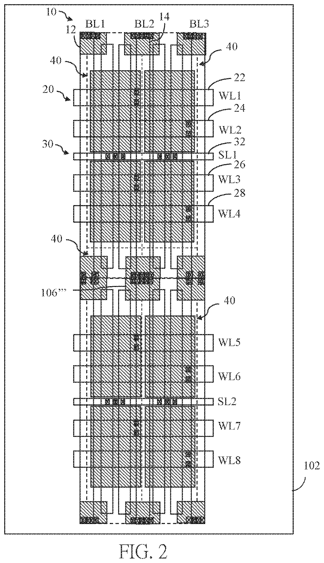
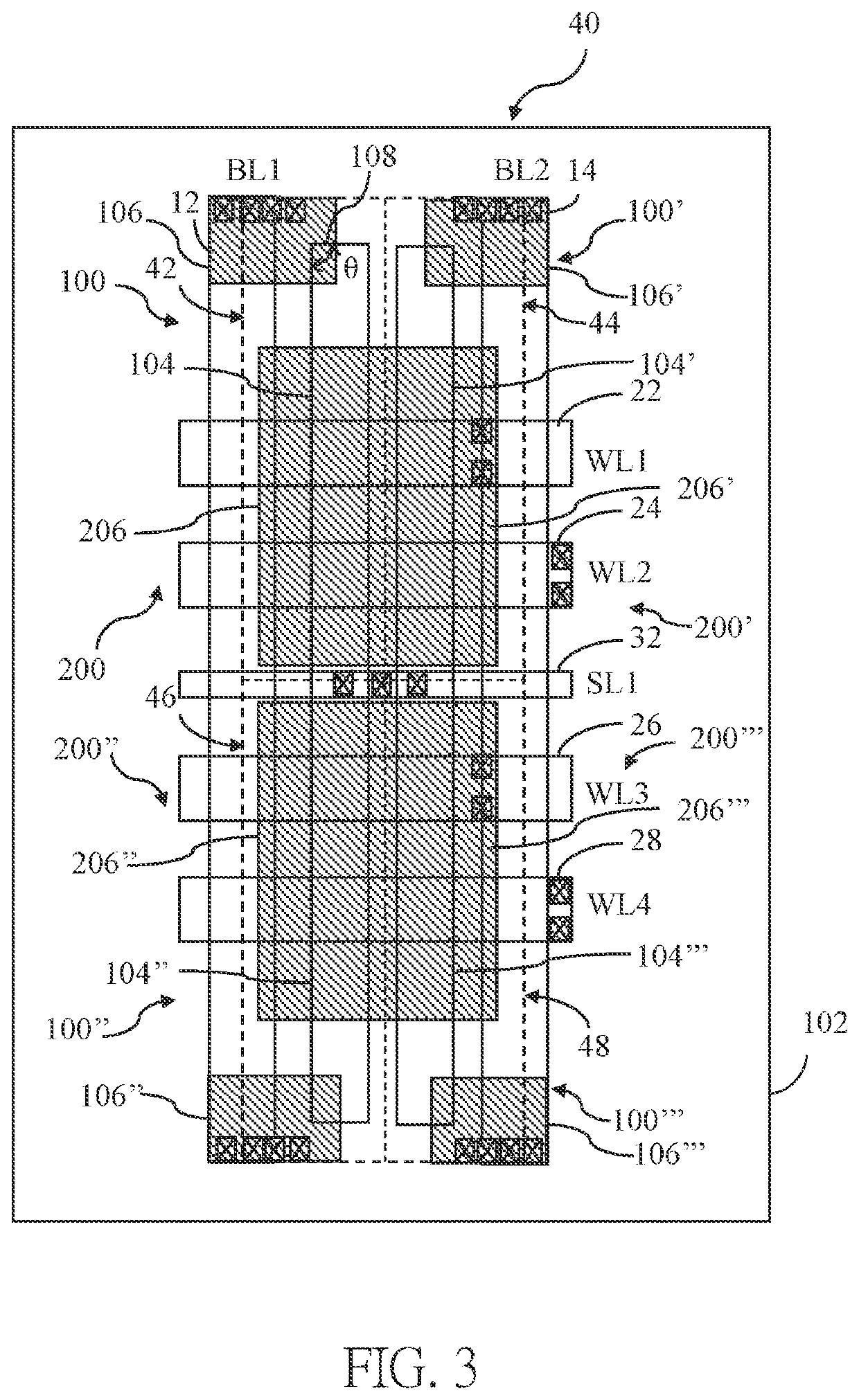
[0014]Please refer to FIG. 2. The low-cost and low-voltage anti-fuse array provided by the embodiment of the present invention comprises a plurality of parallel bit-lines 10. The bit-lines 10 comprises the bit-lines BL1-BL3, wherein the bit-line BL1 is further defined as the first bit-line 12, and the bit-line BL2 is further defined as the second bit-line 14. There is also a plurality of parallel word-lines 20 perpendicular to the bit-line 10, including the word-lines WL1-WL8, wherein the word-lines WL1, WL2, WL3 and WL4 are defined as the first word-line 22, second word-line 24, third word-line 26 and fourth word-line 28, respectively. There are a plurality of parallel selection-lines 30 parallel to the word-line 20, including the selection-lines SL1 and SL2, wherein the selection-line SL1 is further defined as the first selection-line 32. The above bit-line 10, word-line 20 and selection-line 30 are connected to a plurality of sub-memory array 40. As shown in the figure, four sub-...


PUM


Abstract

A low-cost and low-voltage anti-fuse array includes a plurality of sub-memory arrays. In each sub-memory array, the anti-fuse transistor of all anti-fuse memory cells includes an anti-fuse gate commonly used by other anti-fuse transistors. These anti-fuse memory cells are arranged side by side between two adjacent bit-lines, wherein the anti-fuse memory cells in the same row are connected to different bit-lines, and all anti-fuse memory cells are connected to the same selection-line and different word-lines. The present invention utilizes the configuration of common source contacts to achieve a stable source structure and reduce the overall layout area, and meanwhile minimizes the types of control voltage to reduce leakage current.

Description

BACKGROUND OF THE INVENTION[0001]This application claims priority of Application No. 109143386 filed in Taiwan on 9 Dec. 2020 under 35 U.S.C. § 119; the entire contents of all of which are hereby incorporated by reference.FIELD OF THE INVENTION[0002]The present invention relates to an anti-fuse transistor, and more particularly to a low-cost and low-voltage anti-fuse array.DESCRIPTION OF THE PRIOR ART[0003]The anti-fuse transistor mainly uses a capacitive method to add a dielectric layer between two conductors. When writing is performed, a bias is applied to the conductors at both ends in order to make the dielectric layer breakdown and therefore being punctured through. After the writing is done, the resistance value of anti-fuse will decrease. With the rapid development of integrated circuits, the size of components tends to have a reduced design. In recent years, using MOS components to make anti-fuse transistors has been developed. The writing method thereof is mainly substrated...

Claims


Application Information

Patent Timeline
Patent Type & Authority Patents(United States)
IPC IPC(8): H01L27/112
CPCH01L27/11206G11C17/16H10B20/20H01L27/0207H01L23/5252
Inventor HUANG, WEN-CHIENHUANG, YU TINGWU, CHI PEI
Owner YIELD MICROELECTRONICS CORP
Why Eureka
Try Eureka