

Method for fabricating complementary metal oxide semiconductor (CMOS) devices on a mixed bulk and silicon-on-insulator (SOI) substrate
a technology of complementary metal oxide semiconductor and soi substrate, which is applied in the direction of semiconductor devices, electrical equipment, transistors, etc., can solve the problems of trench capacitor dram devices, which are typically built on bulk silicon substrates, and many devices cannot be easily built on so substrates
- Summary
- Abstract
- Description
- Claims
- Application Information
AI Technical Summary
Benefits of technology
Problems solved by technology
Method used
Image

Examples
first embodiment
[0029] First Embodiment
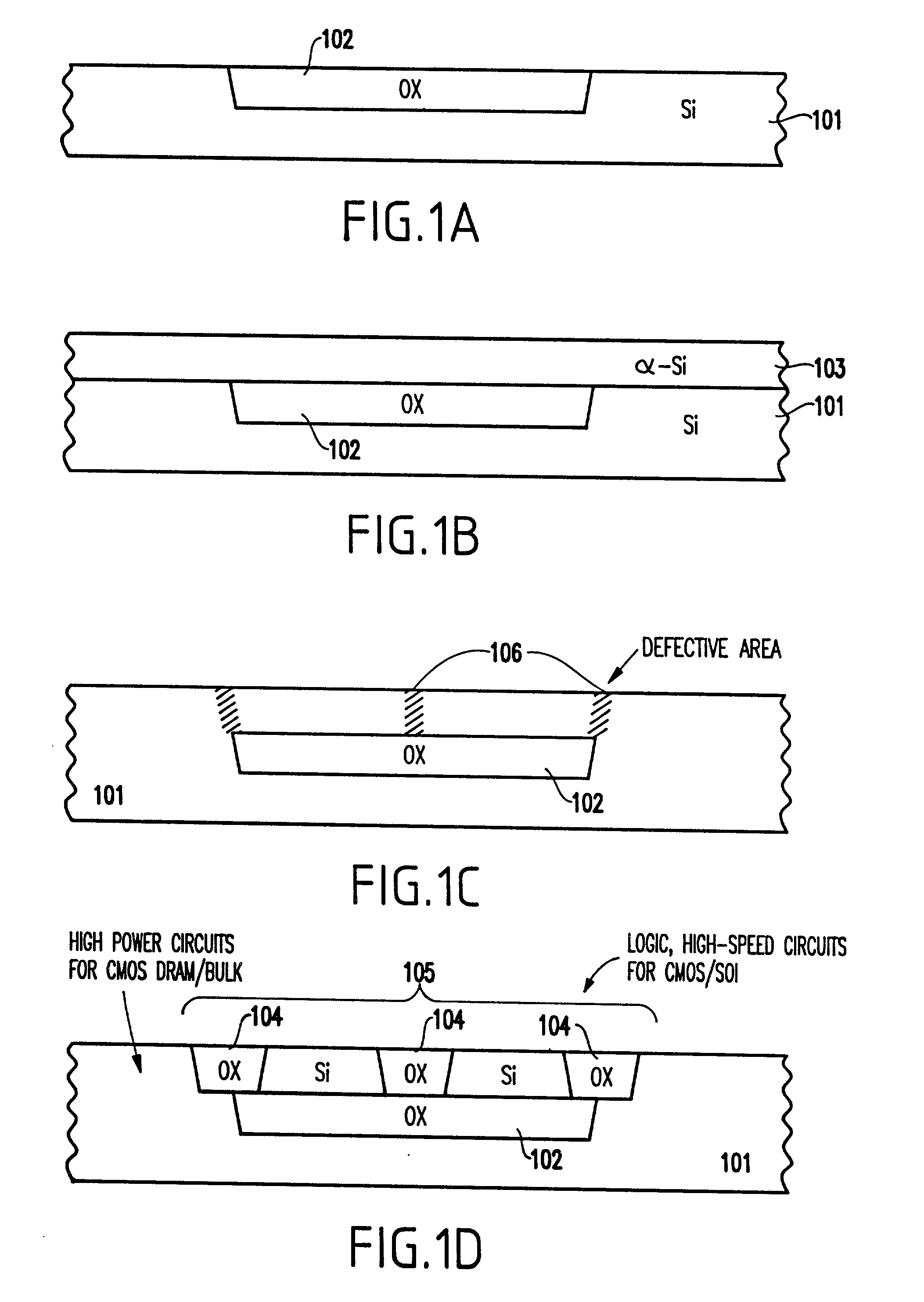
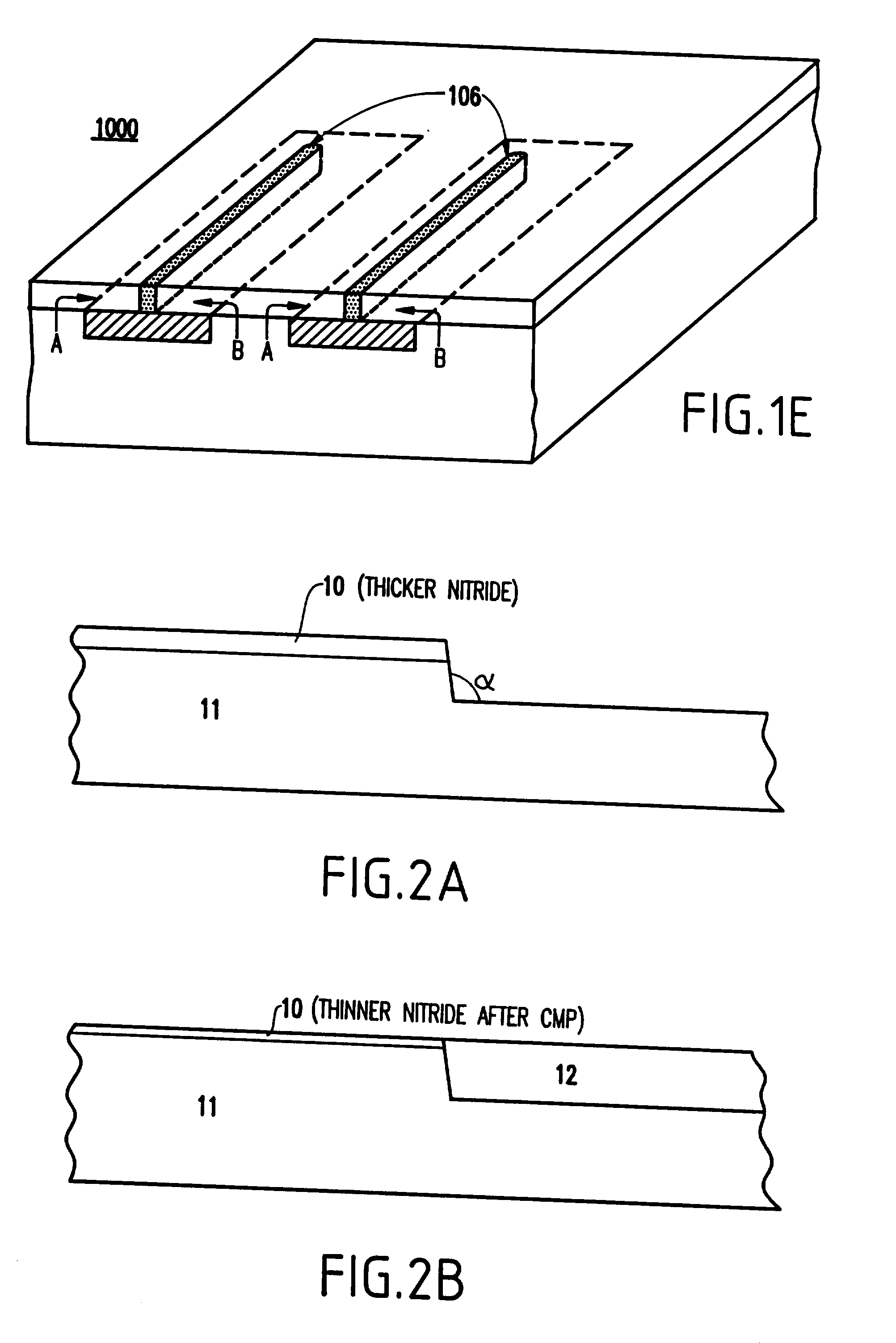
[0030] FIGS. 1A-1D illustrate process of forming a substrate for mixed SOI and bulk applications according to a first embodiment of the present invention. Basically, this process shows how to form a local SOI structure in the bulk substrate including isolation and defect removal steps on the SOI silicon layer.
[0031] In FIG. 1A, a buried oxide layer 102 is processed (using the method described above) on a single crystal silicon substrate 101. Specifically, a shallow groove is formed in the silicon bulk substrate 101, and is filled with an oxide layer. Preferably, the groove has dimensions of about 2 .mu.m to about 10 .mu.m in width, and 1000 .ANG. to 5000 .ANG. in height / thickness.
[0032] Thereafter, as shown in FIG. 1B, an amorphous silicon layer 103 is formed (e.g., deposited) over the oxide 102 and silicon layer 101.
[0033] In FIG. 1C, a process is performed to crystalize the amorphous silicon layer using the single silicon crystal substrate as the seeding. Al...
second embodiment
[0056] Second Embodiment
[0057] Referring to FIGS. 4A-4D, a method according to a second embodiment of the present invention will be described. A difference between the second embodiment is not planarized as in the first embodiment, and thus is not believed to be as preferred as the first embodiment. However, processing costs are reduced with the second embodiment.
[0058] In FIG. 4A, a dielectric (e.g. oxide, nitride) 402 is deposited to a thickness of about 500 .ANG. to about 3000 .ANG., and more preferably to about 1000 .ANG.. Then, the dielectric 402 is patterned through a dry etch or the like. The corner of the patterned dielectric is rounded by dipping in a buffered hydrofluoric (BHF) solution. The rounded corner of the dielectric layer will improve the silicon quality later in the subsequent lateral over-grown epitaxial process.
[0059] As shown in FIG. 4B, an epitaxial lateral over growth is performed in a manner known in the art. Arrow A shows the vertical growth and arrows B il...
PUM
| Property | Measurement | Unit |
|---|---|---|
| thickness | aaaaa | aaaaa |
| width | aaaaa | aaaaa |
| width | aaaaa | aaaaa |
Abstract
Description
Claims
Application Information