Liquid crystal display device implementing improved electrical lines and the fabricating method

a technology of liquid crystal display and electrical lines, applied in non-linear optics, instruments, optics, etc., can solve the problems of increased material cost of lcd device, difficult to repair against drive ic or terminal lines troubles of lcd panel, and difficulty in installing drive ic on the above-mentioned pcb

Inactive Publication Date: 2001-10-04
LG DISPLAY CO LTD
View PDF1 Cites 47 Cited by
  • Summary
  • Abstract
  • Description
  • Claims
  • Application Information

AI Technical Summary

Problems solved by technology

When the drive IC has a great number of leads, it is difficult to install the drive IC on the above-mentioned PCB.
In addition, when the COG method is adopted for the LCD panel, it is difficult to repair a

Method used


Image

  • Liquid crystal display device implementing improved electrical lines and the fabricating method
  • Liquid crystal display device implementing improved electrical lines and the fabricating method
  • Liquid crystal display device implementing improved electrical lines and the fabricating method

Examples


first preferred embodiment

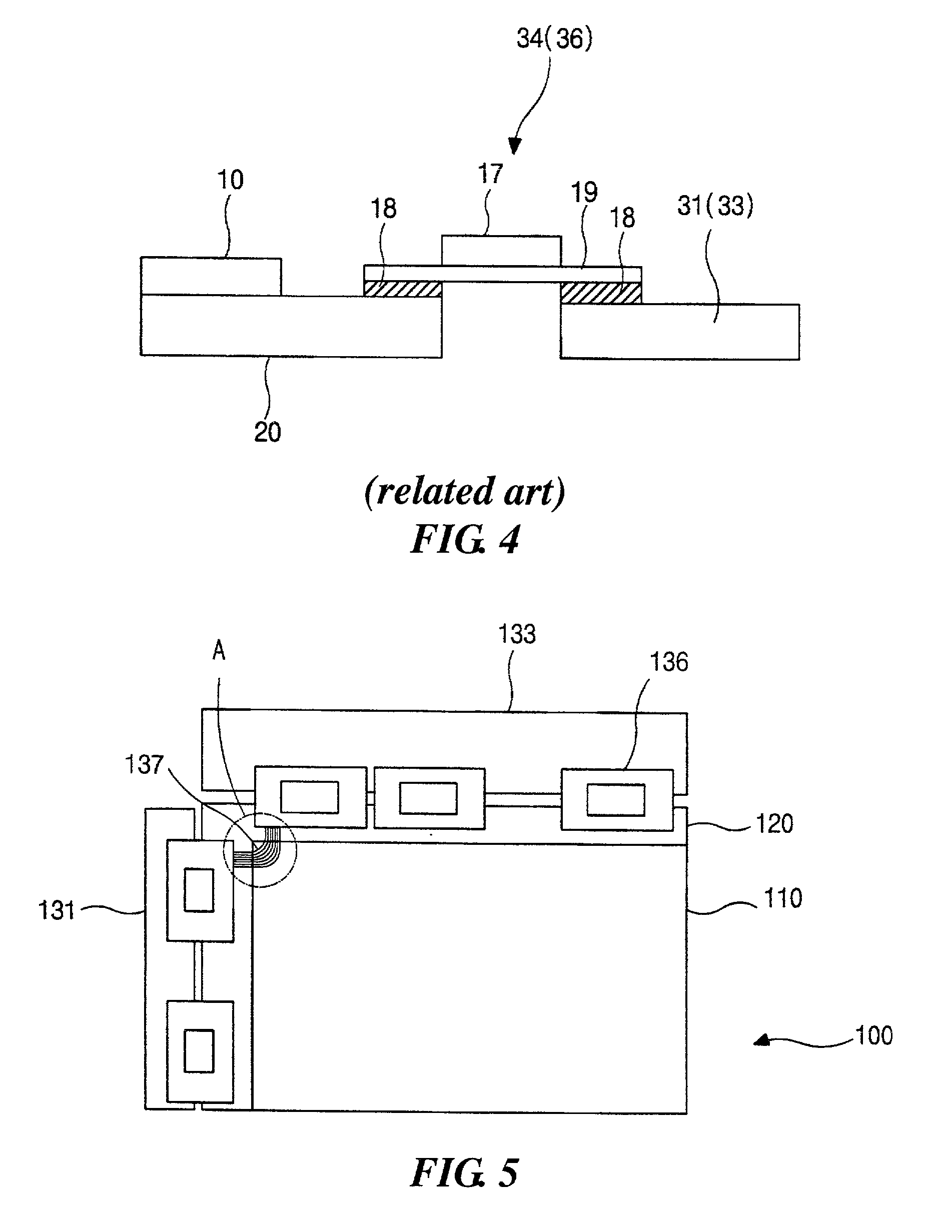
[0057] FIG. 5 is a plane view of a LCD device according to the first preferred embodiment of the present invention.

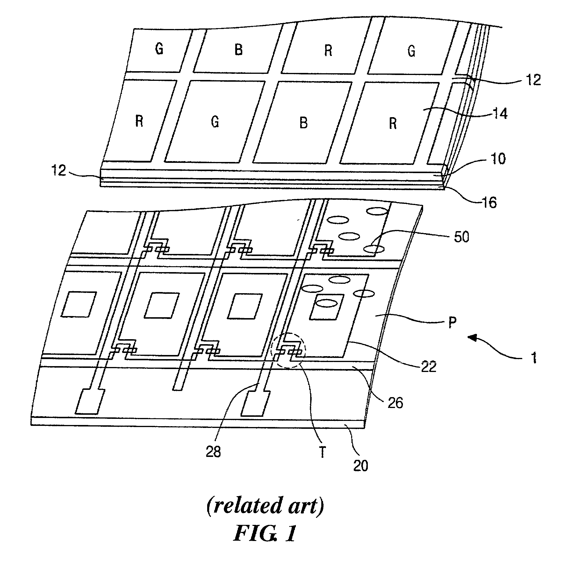
[0058] As shown, an upper substrate 110 is positioned over a lower substrate 120 with a liquid crystal (not shown) interposed between the upper and lower substrates 110 and 120. A sealant 141 shown in FIG. 6 is used to attach the lower and upper substrates 120 and 110. Around edges of the lower substrate 120, gate and source PCBs 131 and 133 are positioned. Gate and source TCPs 134 and 136 electrically connect, respectively, the gate and source PCBs 131 and 133 with a LCD panel 100 including the upper and lower substrates 110 and 120. A gate transmitting wires 137 electrically connects the gate TCP 134 with the source TCP 136 such that the source PCB 133 is electrically connected with the gate PCB 131. The gate transmitting wires 137 are preferably selected from a group consisting of aluminum (Al), molybdenum (Mo), chromium (Cr), alloys thereof and the like.

[0059] FIG. ...

second preferred embodiment

[0065] The second preferred embodiment of the present invention provides a repair wire to repair a short line occurring in the gate transmitting wires provided by the first preferred embodiment of the present invention.

[0066] As shown in FIG. 8, over the gate transmitting wires 137, the repair wire 142 is formed with an insulating layer (not shown) interposed between the gate transmitting lines 137 and the repair wire 142. The repair wire 142 is inwardly spaced apart from the sealant 141 and overlaps two different portions of each gate transmitting wire 137. When a last gate transmitting wire 137a has a short line at a portion "E", the repair wire 142 and the last gate transmitting wire 137a are welded together at their first and second cross points 145 and 147 using a laser and the like. By the above-mentioned repair, the voltage signal is transmitted again via the repair wire 142. The last gate transmitting wire 137a is only an example. When the other of the gate transmitting wire...

third preferred embodiment

[0067] In a scribing and breaking process to separate at least two LCD panels independently from each other, a large sized upper substrate is scribed and broken by force into a plurality of the upper substrates 110 such that a plurality of the LCD panels are fabricated. The third preferred embodiment provides repair wires to repair the gate transmitting wires 137 that are broken in the above-mentioned scribing and breaking process.

[0068] Now, with reference to FIG. 9, the third preferred embodiment is explained.

[0069] As shown, adjacent to each gate pad 128 and each source pad 130, a gate dummy pad 157b and a source dummy pad 157a are formed respectively. Across the source pads 130 and the source dummy pads 157a, a first repair wire 150a is formed with an insulating layer (not shown) interposed between the pads and the repair wire. Similarly, a second repair wire 150b is formed across the gate pads 128 and the gate dummy pads 150a with the insulating layer interposed between the pad...


PUM


Abstract

The present invention discloses a liquid crystal display device, including upper and lower substrates with a liquid crystal layer interposed therebetween; a sealant between the upper and lower substrates; a plurality of source and gate pads on the lower substrate; a plurality of gate and data lines on the lower substrate, each gate line being electrically connected with the corresponding gate pad, each data line being electrically connected with the corresponding source pad; a gate insulating layer between the gate lines and the data lines; a source PCB electrically connected with the plurality of source pads; a gate PCB electrically connected with the plurality of gate pads; and a plurality of transmitting wires on the lower substrate, the transmitting wires being electrically connected with the gate and source pads across the sealant such that the source PCB is electrically connected with the gate PCB. The liquid crystal display device further includes a repair wire to repair the gate transmitting wires, and dummy patterns to protect the gate transmitting wires from a mechanical damage of a scribing and breaking force.

Description

CROSS REFERENCE[0001] This application claims the benefit of Korean Patent Application No. 1999-67851, 2000-18093, and 2000-29104 respectively filed on Dec. 31, 1999, Apr. 7, 2000, and May 29, 2000 under 35 U.S.C. .sctn. 119, the entirety of which is hereby incorporated by reference.[0002] 1. Field of the Invention[0003] The present invention relates to a liquid crystal display (LCD) device, and more particularly, to a liquid crystal display device implementing improved configuration of electrical lines and a fabricating method thereof.[0004] 2. Description of Related Art[0005] A typical liquid crystal display device uses optical anisotropy and polarization properties of liquid crystal molecules. The liquid crystal molecules have a definite orientational order in arrangement resulting from their thin and long shapes. The arrangement direction of the liquid crystal molecules can be controlled by supplying an electric field to the liquid crystal molecules. In other words, as the arran...

Claims


Application Information

Patent Timeline
IPC IPC(8): G02F1/13
CPCG02F1/1309G02F1/13452
Inventor PARK, SUNG-ILYOUN, WON-GYUNSONG, IN-DUKKWON, KEUK-SANGBANG, YOUN-IK
Owner LG DISPLAY CO LTD
Why Eureka
Try Eureka