Power inserter configuration for wireless modems

Inactive Publication Date: 2001-11-01
XENOGENIC DEV LLC
64 Cites 11 Cited by

AI-Extracted Technical Summary

Problems solved by technology

Even though cable access provides much greater performance than traditional telephone modem connections, the bandwidth is still not sufficient to provide high-speed access to a large nu...

Abstract

A wireless modem contains a power inserter circuit along with the traditional modem components. The power inserter circuit isolates the modem components from DC power that is inserted on the coaxial cable to a transverter. One embodiment of the present invention provides for a wireless modem that contains separate power connections for the modem components and the transverter. Another embodiment of the present invention provides for one power connection for the wireless modem and a DC-to-DC converter for the modem component power. The power source is selected based on the power requirements of the transverter and the DC-to DC-converter converts the input voltage into the voltage level required by the modem components. By incorporating the power inserter within the modem enclosure, power cannot be accidentally inserted into the modem.

Application Domain

Resonant long antennasSubstation equipment +1

Technology Topic

DC-to-DC converterTransverter +5

Image

  • Power inserter configuration for wireless modems
  • Power inserter configuration for wireless modems
  • Power inserter configuration for wireless modems

Examples

  • Experimental program(1)

Example

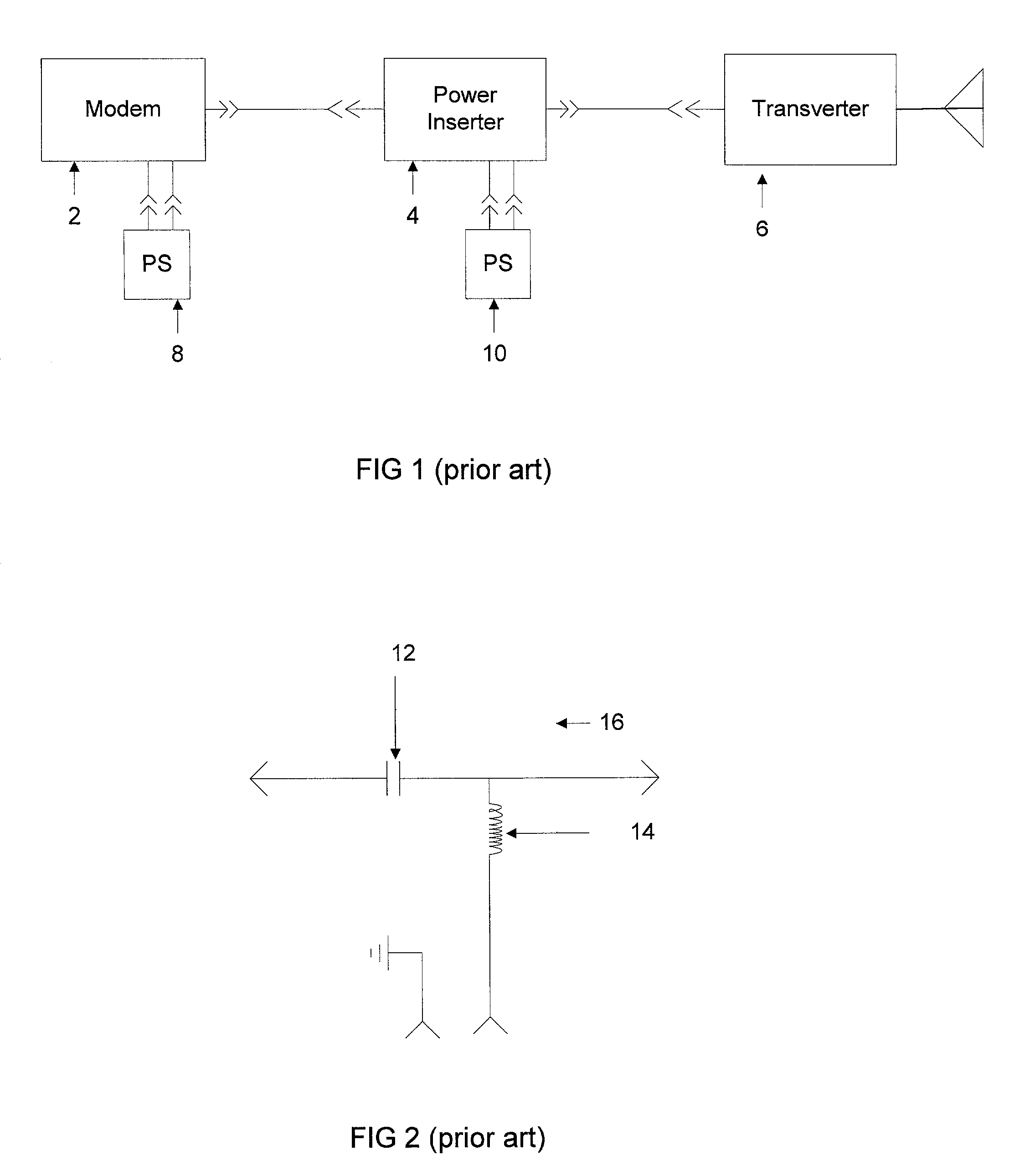
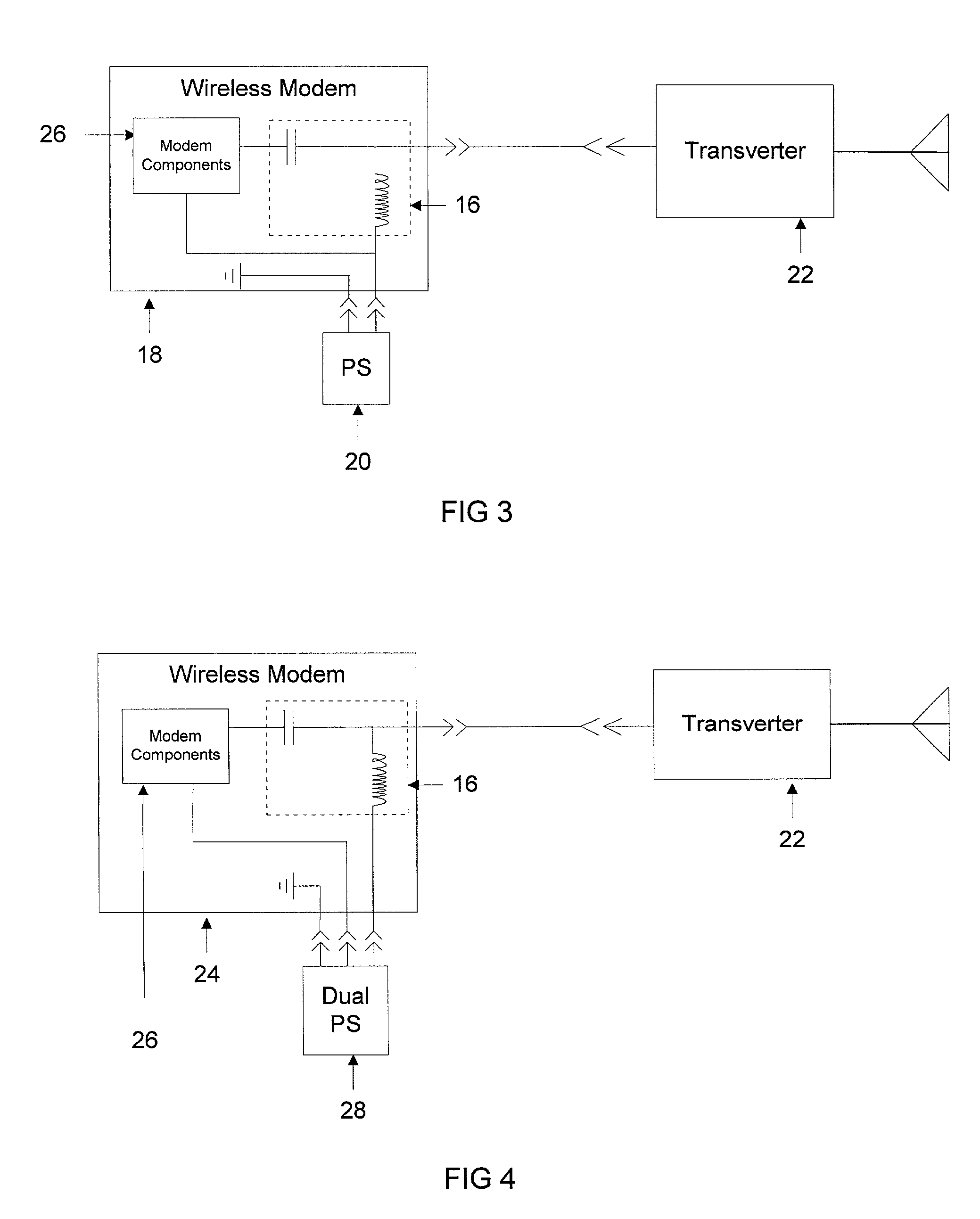
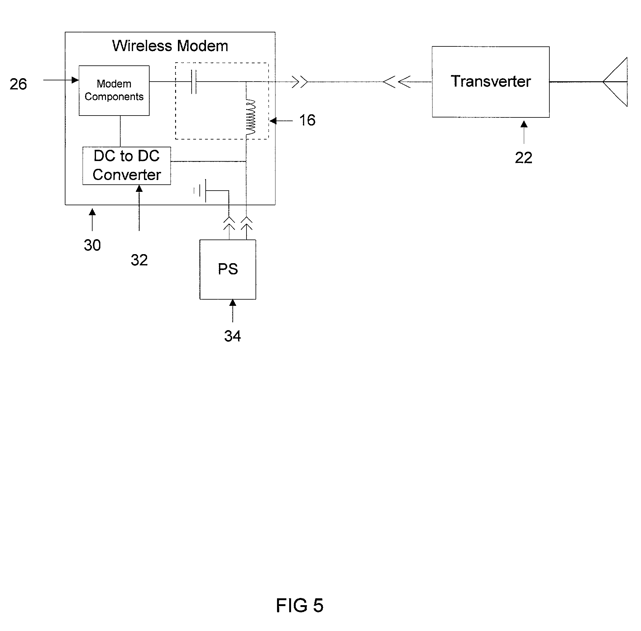
[0015] The following description is provided to enable any person skilled in the art to make and use the invention and sets forth the best modes contemplated by the inventor for carrying out the invention. Various modifications, however, will remain readily apparent to those skilled in the art, since the basic principles of the present invention have been defined herein specifically to provide a power inserter configuration for wireless modem systems.
[0016] According to the present invention, a wireless modem 18 includes a power inserter circuit 16 to provide electrical power to a transverter 22 via a coaxial cable, as illustrated in FIG. 3. The wireless modem 18 also contains modem components 26, which is the circuitry traditionally found in modems known by those skilled in the art. The coaxial cable also provides a signal path for data transfer between the wireless modem 18 and the transverter 22. The power inserter circuit 16 shields the output of the modem components 26 from DC power insertion from a power source 20. Also, the power inserter circuit 16 shields the power source 20 from IF energy from the output of the modem components 26. Thus, the present invention eliminates the possibility of accidental voltage injection into the wireless modem 18.
[0017] In practical use, the transverter 22 may require different voltages depending on the manufacturer of the transverter 22. Typically, the voltages required by the transverter 22 range from 12 to 48 Volts. Unacceptable performance may result if too low of a voltage is used for the transverter 22. A voltage higher than that required by the transverter 22 may result in overheating or other damage to the transverter 22. The varying voltage levels required by the transverter 22 pose a problem because the wireless modem 16 and the transverter 22 may not use the same voltage. Thus, it would be desirable to have a more universal solution.
[0018] One solution is to require all transverter manufacturers to include a DC-to-DC converter in all transverters to achieve a fairly wide input voltage tolerance. This solution is not very desirable because it would require all transverter manufacturers to cooperate and agree on the same standards.
[0019] A second approach is illustrated in FIG. 4. Here, a dual power source 28 has three connectors for a wireless modem 24: 1) a voltage connector for the modem components 26, 2) a voltage connector for the transverter 22, and 3) a common ground connector. This configuration supplies one voltage level to the modem components 26 and a separate voltage level for the transverter 22 by way of the power inserter circuit 16. This configuration eliminates the need to alter the transverter 22 voltage input. However, having a third connector on the dual power source 28 and the wireless modem 24 is more costly. Also, this configuration is inefficient because it requires a user to obtain a dual power source 28 that matches the required voltage levels of the wireless modem 24 and the transverter 22.
[0020] A third approach is illustrated in FIG. 5. A wireless modem 30 includes a DC-to-DC converter 32 to allow the wireless modem 30 to accept a wide range of input voltages. In this manner, a power source 34 is selected according to the voltage level required by the transverter 22. If the voltage required by the transverter 22 is not the same as the voltage required by the modem components 26, the DC-to-DC converter 32 converts the input voltage to the voltage level required by the modem components 26 for normal operation. Thus, the present invention eliminates a separate power connection and/or supply for the power inserter circuit 16, additional connections between the wireless modem 30 and the transverter 22, and the possibility of accidental power injection into the output of the modem components 26.
[0021] Those skilled in the art will appreciate that various adaptations and modifications of the just-described preferred embodiment can be configured without departing from the scope and spirit of the invention. Therefore, it is to be understood that, within the scope of the appended claims, the invention may be practiced other than as specifically described herein.

PUM

no PUM

Description & Claims & Application Information

We can also present the details of the Description, Claims and Application information to help users get a comprehensive understanding of the technical details of the patent, such as background art, summary of invention, brief description of drawings, description of embodiments, and other original content. On the other hand, users can also determine the specific scope of protection of the technology through the list of claims; as well as understand the changes in the life cycle of the technology with the presentation of the patent timeline. Login to view more.
Why Eureka
Try Eureka