Power amplifier with close-loop adaptive voltage supply

a voltage supply and power amplifier technology, applied in the direction of amplifiers, amplifiers with semiconductor devices only, amplifiers with semiconductor devices, etc., can solve the problems of shortening the handset talk time, increasing the current consumption of additional active components, and reducing the current consumption, so as to save battery life and reduce current consumption

Inactive Publication Date: 2007-08-09
SEMICON COMPONENTS IND LLC
View PDF7 Cites 89 Cited by
  • Summary
  • Abstract
  • Description
  • Claims
  • Application Information

AI Technical Summary

Benefits of technology

[0015] The above limitations of the prior art are avoided and other advantages are provided by the present invention. The present invention provides for, at least, a two-stage power amplifier, where the bias voltage applied to the power amplifier varies dynamically wi

Problems solved by technology

The additional active components demand higher current consumption which, inevitably, shortens the battery life.
On the other hand, wireless service providers and consumers demand long handset talk time from the next generation handsets.
The power added efficiency (PAE) of the conventional power amplifiers usually drops off rapidly under such backoff power operation, resulting in higher current draw coupled with excessive linearity margin.
As known to those skilled in the art, the excessive linearity margin can be trade-off for low current consumption in power amplifiers.
Although, this improves overall efficiency, it remains inefficient at other power levels, and, as mobile devices proliferate, battery life is becoming more important in the competitive market.
However, the coupling loss (typically through a resistor or a current mirror) in the bias line would cause voltage drop especially under high current operation, reducing the bias voltage available to the power amplifier and resulting in performance

Method used


Image

  • Power amplifier with close-loop adaptive voltage supply
  • Power amplifier with close-loop adaptive voltage supply
  • Power amplifier with close-loop adaptive voltage supply

Examples


Embodiment Construction

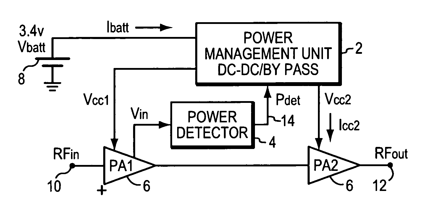
[0032]FIG. 1 is a block diagram of a system employing the present invention and includes a power management unit 2, a power detector 4, a 3.4V battery 8, and two power amplifiers 6, PA1 and PA2. Consider the circuit of FIG. 1 is part of a handset that has just been turned on and has received a new RF control signal from a base station. In this case, the RFin signal 10 is changed to a level such that the circuit of FIG. 1 will deliver the optimum, pre-determined output power at the RFout signal 12 which corresponds to that particular RFin signal level. Vin is an RF signal sensed from the output of the first power amplifier PA1 that is input to the power detector 4. The power detector 4 outputs a DC voltage Pdet to a DC to DC converter in the power management unit 2. The DC to DC converter responds by providing optimum Vcc1 and Vcc2 to PA1 and PA2, respectively. In most instances Vcc1 equals Vcc2, but in other application these voltages may be different. The circuitry is powered from ...


PUM


Abstract

A two- (or multi) stage power amplifier receives a variable RF input signal, and outputs an optimized. RF output signal from, for example, a mobile handset. The output power level from the handset is predetermined, as known in the art, by the received control signal from a base station. The first power amplifier stage amplifies the variable RF input signal and outputs an RF signal, Vin, to a power detector circuit and an RF signal to the second or next amplifier stage. The power detect circuit amplifies the Vin signal and rectifies that signal with a linearly biased diode and provides a detect signal to a DC to DC converter. The converter responds by providing an optimum voltage bias, which is linearly related to the DC voltage detect signal from the power detector, to the output stage, and, if desired, to the first and/or other stages of the power amplifier that optimizes the output power level while meeting the required linearity specification. The battery current consumption is optimized through this automatic, dynamically control of the supply voltage for the power amplifier at each output power level through the DC to DC converter.

Description

BACKGROUND OF THE INVENTION [0001] 1. Field of the Invention [0002] The present invention relates to power amplifiers and, more particularly, to power amplifiers used in battery powered mobile handsets, and even more particularly to optimizing current use in such power amplifiers over a range of output power levels. [0003] 2. Background Information [0004] Mobile handsets for wireless communication have become highly integrated to support new features such as multi-standard operation, camera, color display and high data rate transmission. The additional active components demand higher current consumption which, inevitably, shortens the battery life. On the other hand, wireless service providers and consumers demand long handset talk time from the next generation handsets. Hence, there is a constant need to reduce power consumption of the handset components in order to extend battery life. [0005] The RF power amplifier is one of the main current consuming parts within handsets. Signal...

Claims


Application Information

Patent Timeline
IPC IPC(8): H03F3/04
CPCH03F1/0227H03F2200/507H03F2200/504H03F2200/465
Inventor HAU, GARYBEALO, PETER
Owner SEMICON COMPONENTS IND LLC
Why Eureka
Try Eureka