Dielectric filter, dielectric duplexer, communication system, and method of producing dielectric filter
- Summary
- Abstract
- Description
- Claims
- Application Information
AI Technical Summary
Benefits of technology
Problems solved by technology
Method used
Image

Examples
first embodiment
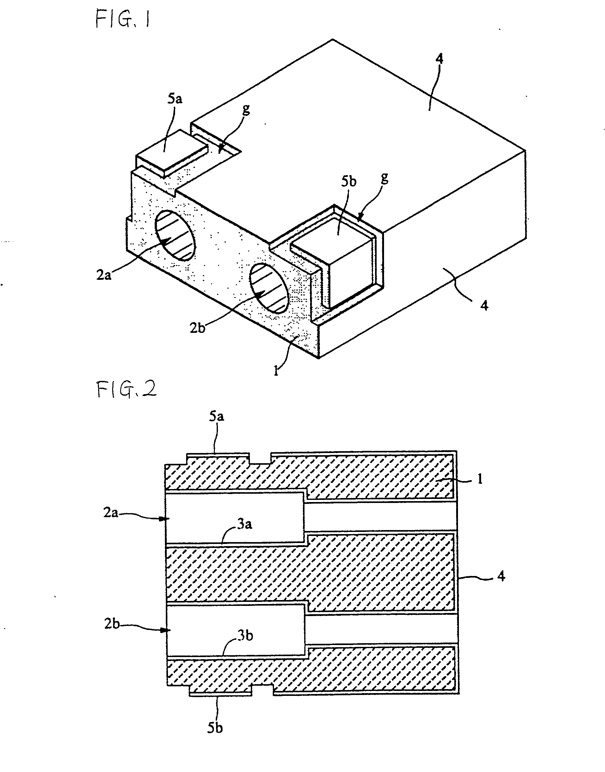
[0033] Hereinbelow, the structure of a dielectric filter will be illustrated with reference to FIGS. 1 to 3B.
[0034] FIG. 1 is a perspective view of the dielectric filter according to the first embodiment, FIG. 2 is a central cross-sectional view of the dielectric filter, and FIGS. 3A and 3B are a side view and a top view of the dielectric filter, respectively. As shown in the figures, inner-conductor holes 2a and 2b whose internal surfaces are coated with inner conductors 3a and 3b, respectively, are provided in a dielectric block 1 which is substantially a rectangular parallelepiped, and input / output electrodes 5a and 5b and an outer conductor 4 are formed on external surfaces of the dielectric block 1. The inner-conductor holes 2a and 2b penetrate from a first end surface of the dielectric block 1 to a second end surface facing thereto, as shown in FIG. 2. The first end surface of the dielectric block 1 is an open surface forming an open-circuited end of each inner conductor, and...
second embodiment
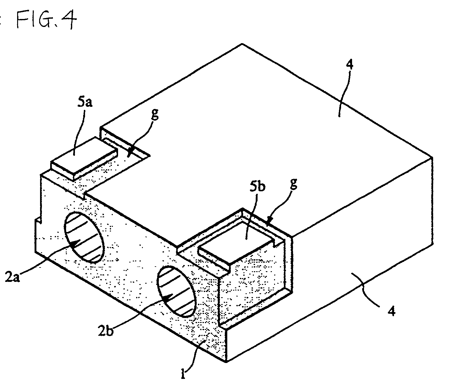
[0045] Next, the structure of a dielectric filter will be described with reference to FIGS. 4, 5A, and 5B.
[0046] FIG. 4 is a perspective view of the appearance of the dielectric filter according to the second embodiment, and FIGS. 5A and 5B are a side view and a top view of the dielectric filter, respectively. The dielectric filter in the second embodiment is different from that shown in FIG. 1 in that the input / output electrodes 5a and 5b are provided only on a top surface (mounting surface) of a dielectric block 1, and only gap portions are provided on side surfaces thereof. The structure in other portions is similar to that in the first embodiment.
[0047] In the structure, the dielectric filter 1 functions as a filter which comprises two resonators coupled to the outside by electrostatic capacitance and has band-pass characteristics.
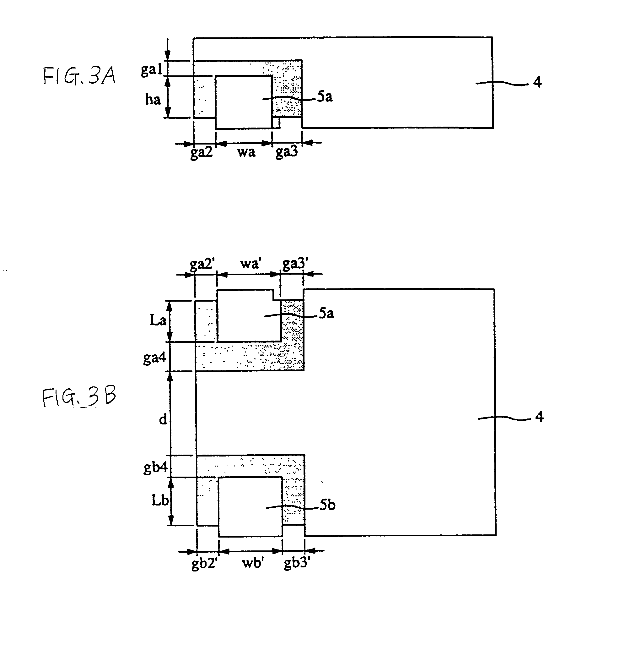
[0048] FIGS. 5A and 5B are diagrams showing the dimensions of gap portions between input / output electrodes 5a and 5b and an outer conductor 4 and dim...
third embodiment
[0052] Next, a description is given of some examples of a dielectric filter with reference to FIGS. 6A-6C.
[0053] FIGS. 6A to 6C are side views of the dielectric filter. Because the structures of the other surfaces of the dielectric block are similar to those shown in FIG. 1 to FIGS. 3A and 3B, the description thereof is omitted.
[0054] In an example shown in FIG. 6A, a cut depth of a gap portion g between an input / output electrode 5a and an outer conductor 4 is different from that in a gap portion g'. In an example shown in FIG. 6B, a gap portion g' is deeper than the gap portion g. The degree of change in the electrostatic capacitance generated between the input / output electrode 5a and an inner conductor differs from the degree of change in the electrostatic capacitance generated between the input / output electrode Sa and the outer conductor 4 depending on the change in the cut depth of the gap portion. Accordingly, in the ge structures, the cut depth of the gap portion is partly ch...
PUM
 Abstract
Description
Claims
Application Information
 - R&D
- Intellectual Property
- Life Sciences
- Materials
- Tech Scout
- Unparalleled Data Quality
- Higher Quality Content
- 60% Fewer Hallucinations
Browse by: Latest US Patents, China's latest patents, Technical Efficacy Thesaurus, Application Domain, Technology Topic, Popular Technical Reports.
© 2025 PatSnap. All rights reserved.Legal|Privacy policy|Modern Slavery Act Transparency Statement|Sitemap|About US| Contact US: help@patsnap.com