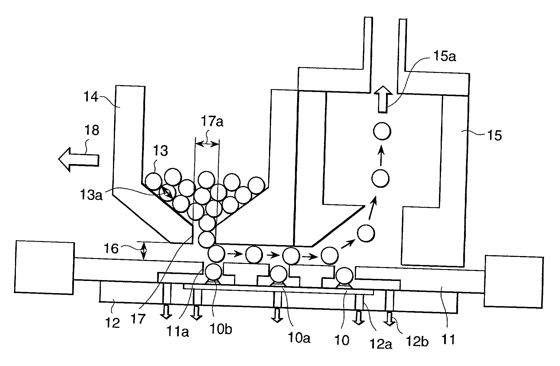
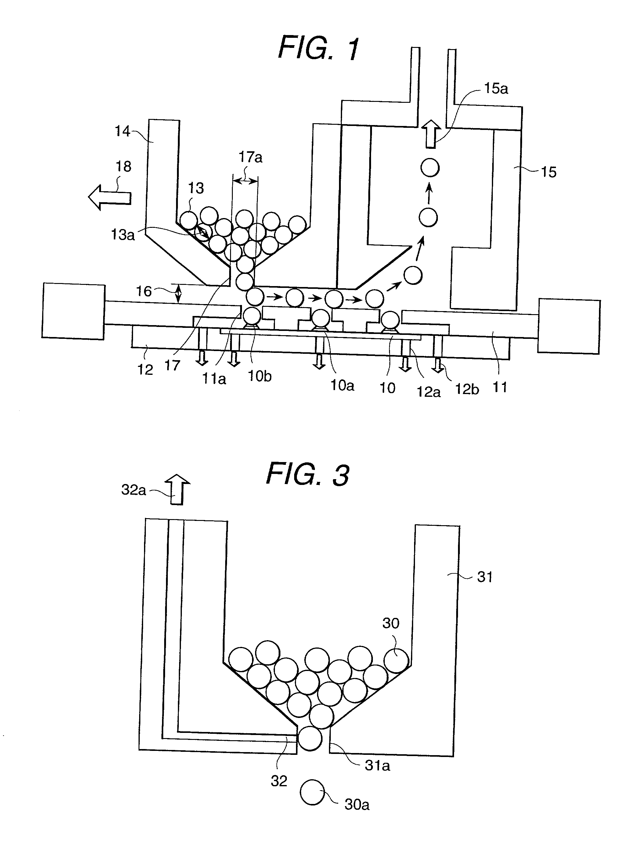
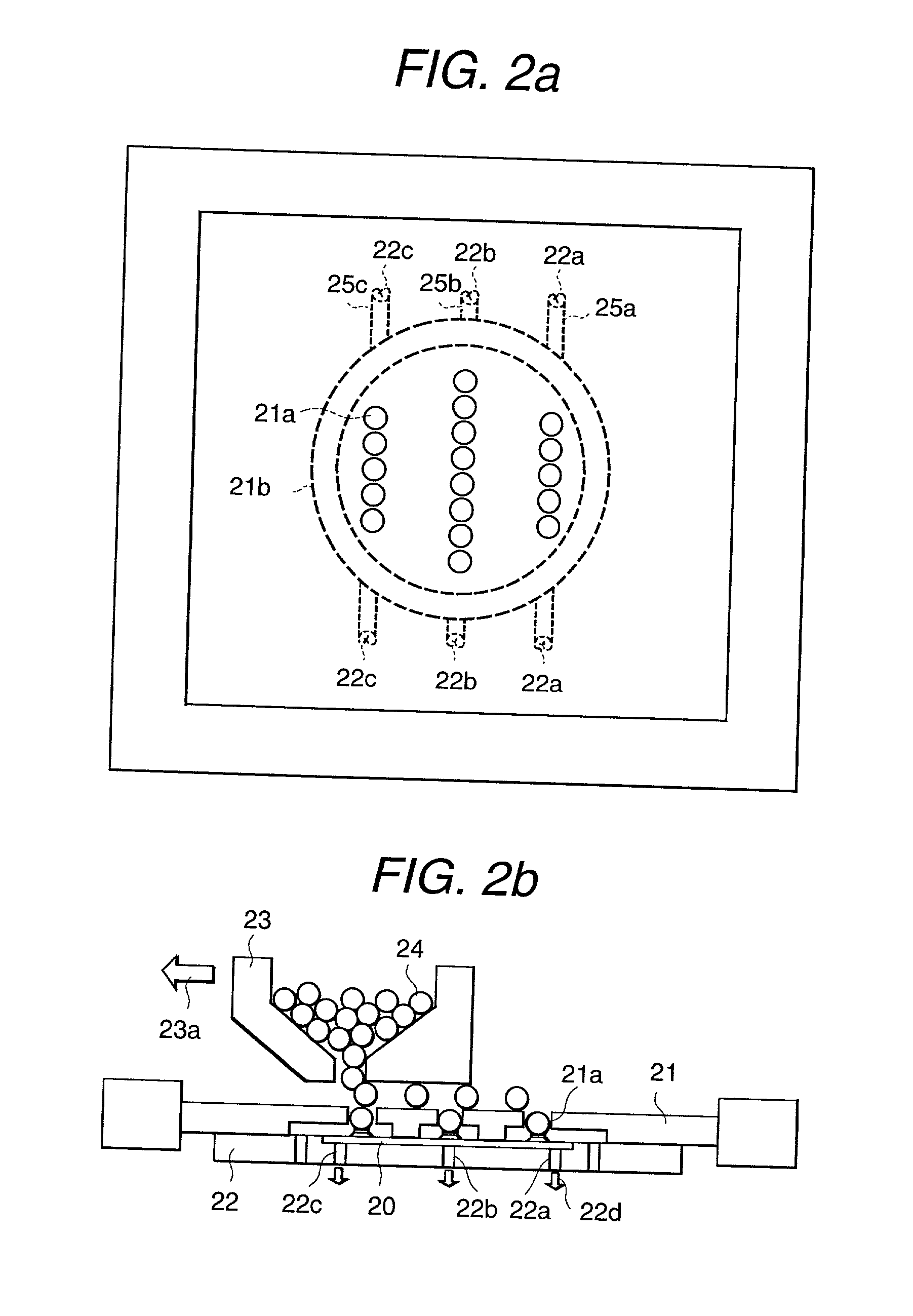
As the IC is being downsized, the conventional plating method is difficult to form bumps having a sufficient volume and further has a problem that the plating time requires a long time.
On the other hand, the conventional printing method has a problem that when the bumps of an IC are connected to a circuit board or the like, it is difficult to connect all of the bumps correctly because deviations occur in the bump volume and the bump height.
Further, the conventional stud bump method has a problem that the
electrically conductive material of the circuit board used for being connected to the bumps is limited because the material of the bumps is gold.
Further, the conventional
solder ball mounting method has the problems that number of balls capable of mounting at a time is only several hundreds and that the ball can not be mounted unless the
diameter of the ball is above 300 .mu.m though the bumps can be formed without deviations in the bump volume and the bump height.
In addition to the above problems, there is a problem that since time required for mounting the
solder ball is approximately 15 seconds / mounting, it takes more than several hours to
mount several tens thousands solder balls and accordingly the productivity is low.
However, the conventional bump forming methods of (Example A) to (Example I) described above have problems as follows.
The first problem of the structure in the conventional bump forming methods is that the conductive particles adhere to each other.
Since the conductive particles adhere onto the surface portion of the mask or the inside of the through holes of the mask, and the supply unit or the
brush, the squeegee or the like by the
static electricity, movement of the conductive particles can not be controlled, and accordingly the conductive particles can not be certainly supplied into the through holes of the mask by the self-weight.
Further, since the conductive particles adhere to halfway positions, in incomplete states, of the though holes of the mask due to the influence of the
static electricity, there occurs a phenomenon that the conductive particles are seized in the tip end portion of the supply unit or the end surface portion of the squeegee to cause damage of the conductive particles.
The second problem of the structure in the conventional bump forming methods is that the conductive particles are apt to be deformed by external forces acting on the conductive particles because the conductive particles are slid on the mask using the squeegee or the
brush, and accordingly the conductive particles can not be certainly inserted into or supplied to the though holes of the mask by the self-weight when the conductive particles are deformed by an amount above a
diameter of the through holes of the mask.
The third problem of the structure in the conventional bump forming methods is that when the mask is removed from the
wafer or the circuit board after putting the many conductive particles into the through holes of the mask, the conductive particles mounted on the electrode portions on the circuit board are apt to drop down due to friction between the inner surface of the though hole of the mask and the conductive particle.
Here, describing on the known technology of Example A described above, since the solder balls are dropped into the through holes of the mask only using the self-weight of the
solder ball, there is a problem that the solder balls are charged and the many solder balls stay and remain at positions other than the through holes of the mask.
In addition to this, there is a problem in that the solder balls introduced into the through holes of the mask are apt to be dropped down by vibration of the mask produced when the circuit board and the mask are turned over.
However, this influence of the vibration is not taken into consideration.
Further, the known technology of Example B does not take into consideration how to put the solder balls into the through holes of the mask.
Further, since the solder balls adhere to halfway positions of the though holes of the mask, there occurs the phenomenon that the solder balls are apt to be chipped by being seized in the corner portion of the box-shaped storing frame.
Further, the conductive particles are apt to be deformed by external forces acting on the conductive particles because the structure is that the conductive particles are slid on the mask using the box-shaped storing frame, and accordingly the conductive particles are difficult to be dropped into the through holes of the mask by the self-weight when the conductive particles are deformed by an amount above a diameter of the through holes of the mask.
Further, since the solder balls adhere to halfway positions of the through holes of the mask by the static
electricity, there occurs the phenomenon that the solder balls are apt to be chipped by being seized in the end portion of the ball hopper or the pressing member.
Further, the conductive particles of the conductive particles are apt to be deformed by external forces acting on the solder balls because the structure is that the conductive particles are slid on the mask using the ball hopper, and accordingly the conductive particles are difficult to be dropped into the through holes of the mask by the self-weight when the conductive particles are deformed by an amount above a diameter of the through holes of the mask.
Further, since the solder balls adhere to halfway positions of the through holes of the mask by the static
electricity, there occurs the phenomenon that the solder balls are apt to be chipped by being caught by the squeegee.
Further, the conductive particles are apt to be deformed by external forces acting on the conductive particles because the structure is that the conductive particles are slid on the mask using the sword-tip-shaped squeegee, and accordingly the conductive particles are difficult to be dropped into the through holes of the mask by the self-weight when the conductive particles are deformed by an amount above a diameter of the through holes of the mask.
The conventional technologies described above have not been practically used because the structure is that the conductive particles are difficult to be dropped into the through holes of the mask due to the influence of the static
electricity and the van der Waar force produced on the surfaces of the conductive particles, and because the problem of producing the damage such as forming chips in the conductive particles can not solved due to the structure that the conductive particles are apt to be caught by the tip end portion of the supply unit such as the hopper or the like.


