Semiconductor integrated circuit device, storage medium on which cell library is stored and designing method for semiconductor integrated circuit

a technology of integrated circuits and semiconductors, applied in logic circuit coupling/interface arrangements, pulse techniques, instruments, etc., can solve the problems of increased consumption power due to leakage current, increased consumption power by leakage current, and large consumption power

Inactive Publication Date: 2002-06-27
RENESAS ELECTRONICS CORP
View PDF0 Cites 156 Cited by
  • Summary
  • Abstract
  • Description
  • Claims
  • Application Information

AI Technical Summary

Benefits of technology

[0020] A second feature of a semiconductor integrated circuit device of the present invention is that when, in a signal path in the semiconductor integrated circuit device, if the path is constructed of only MOSFETs each with a high threshold voltage, a delay is large and a requirement for an operating frequency cannot be satisfied, but if the path is constructed of only MOSFETs each with a low threshold voltage, a margin arises in delay and consumption power due to a leakage current is uselessly increased, then MOSFETs each with a low threshold voltage and MOSFETs each with a high threshold voltage are mixed in a proper manner along the signal path and thereby, a delay which satisfies a requirement for an operating frequency is secured and at the same time a leakage current is suppressed to a minimum.

Problems solved by technology

However, when a threshold voltage is set to an excessively low value, there arise problems that an MOSFET cannot perfectly be turned off due to subthreshold characteristics (tailing characteristics) of the MOSFET, a subthreshold current (hereinafter "leakage current" is used) is increased and thereby consumption power is very large, as described in 1993 Symposium on VLSI Circuits Digest of Technical Papers, pp.
However, in the method that threshold voltages of MOSFETs are uniformly increased in a standby state and those are again uniformly decreased in an active operating state, increase in consumption power due to leakage current cannot be avoided in order to secure a high speed operation in the active operating state.
In this case, however, consumption power by a leakage current is increased and there arises a risk that a required condition posed on consumption power is not met.
That is, an operating speed is lowered and thereby 100 MHz cannot be realized.
That is, it is unavoidable that there exists a path which has the largest delay time, which determines an overall operating speed among paths between a plurality of first circuits.

Method used


Image

  • Semiconductor integrated circuit device, storage medium on which cell library is stored and designing method for semiconductor integrated circuit
  • Semiconductor integrated circuit device, storage medium on which cell library is stored and designing method for semiconductor integrated circuit
  • Semiconductor integrated circuit device, storage medium on which cell library is stored and designing method for semiconductor integrated circuit

Examples


second embodiment

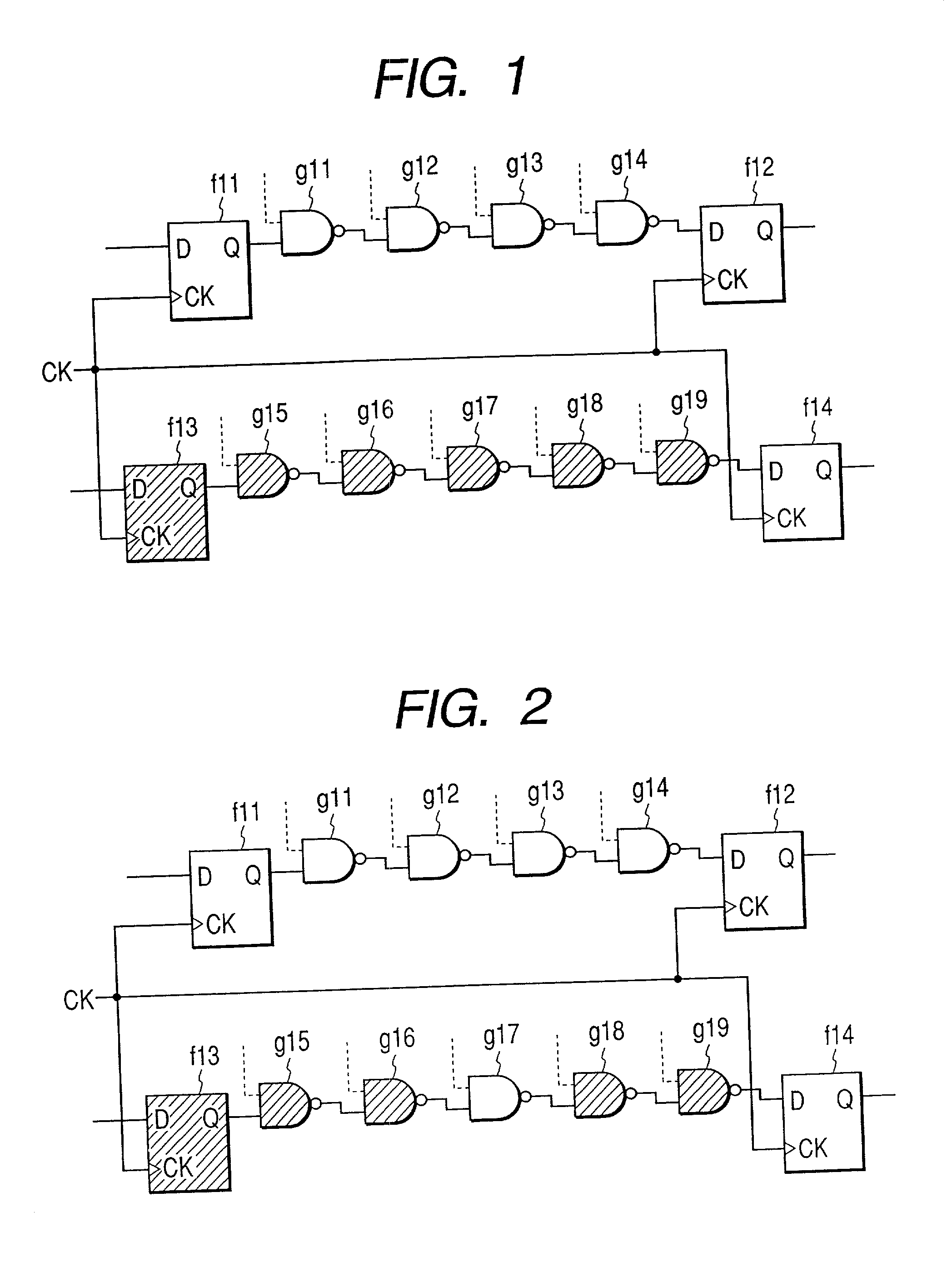
[0068] a logic gate circuit in a semiconductor integrated circuit device of the present invention will be shown using FIG. 2. The circuit of FIG. 2 is absolutely the same circuit as FIG. 1 but only with exception that a logic gate g17 of FIG. 2 is constructed with MOSFETs each with a high threshold voltage. In FIG. 1, all the logic gates along the path from f13 and g15 through g19 to f14 are constructed of MOSFETs each with a low threshold voltage and a delay is 4.8 nsec. It means that there is left a margin of 0.2 nsec in order to operate at an operating frequency. In the case of FIG. 2, when one element constructed of MOSFETs each with a high threshold voltage is mixed in a path from f13 and g15 through g19 to f14, too, a delay can be made to assume 5 nsec and a total leakage current can further be decreased to 33 pA. That is, an essential point of the embodiment shown in FIG. 2 is that MOSFETs with different threshold voltages are mixed in a proper manner even in one signal circu...

third embodiment

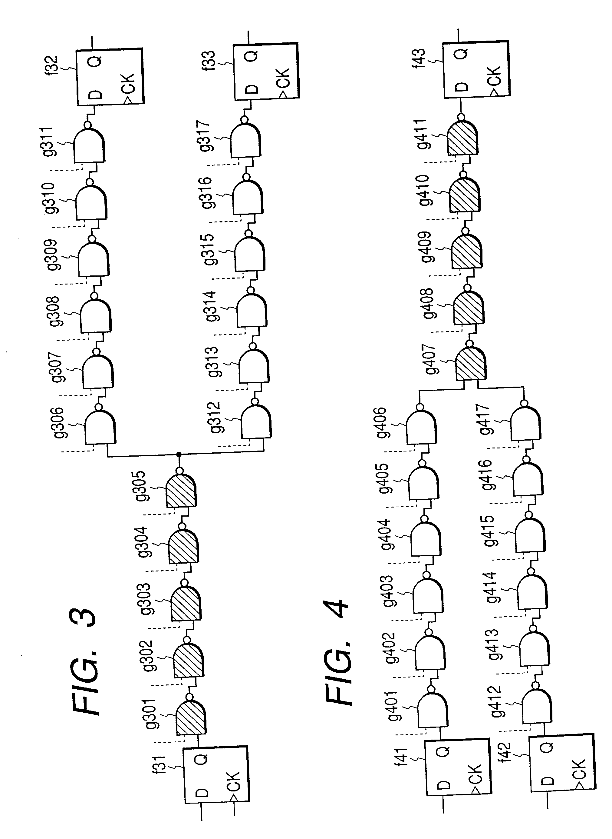
[0069] a logic gate circuit in a semiconductor integrated circuit device of the present invention is shown in FIG. 3. In FIG. 3, the circuit is constructed of flip-flops f31, f32, f33 and logic gates g301 to g317. It is assumed that target delays of the path f31 to f32 and the path f31 to f33 are both 10 nsec. Delays and a leakage current of each element is the same as those of FIGS. 1 and 2. Either of the path from f31 to f32 and the path f31 and f33 is constructed of eleven logic gates and there is a necessity that at least 5 elements among the eleven logic gates are constructed with MOSFETs each with a low threshold voltage in order to realize a delay of 10 nsec.

[0070] When a common portion on both paths from g301 to g305 is constructed with MOSFETs each with a low threshold as shown in FIG. 3, the number of logic gates constructed of MOSFETs each with a low threshold can be minimized in the whole circuit. In this case, a total leakage current is 37 pA. When logic gates other tha...

fourth embodiment

[0071] a logic gate circuit in a semiconductor integrated circuit device of the present invention is shown using FIG. 4. FIG. 4 is constructed of flip-flops f41, f42, f43 and logic gates g401 to g417. Target delays of a path from f41 to f43 and a path from f42 to f43 are both 10 nsec as in FIG. 3. Delays and leakage current of respective elements are same as those in FIGS. 1 to 3. Either of the path extending from f41 to f43 and the path extending from f42 to f43 contains eleven logic gates and there is a necessity that at least five elements among the eleven logic gates have to be constructed of MOSFETs each with a low threshold voltage in order to realize a delay of 10 nsec.

[0072] When the common portion of both paths f407 to g411, as shown in FIG. 4, is constructed of MOSFETs each with a low threshold voltage, the number of logic gates constructed of MOSFETs each with a low threshold voltage is minimized in the whole circuit. In this case, a total current is 37 pA. When logic gat...


PUM


Abstract

Disclosed is a semiconductor integrated circuit device constructed of MOSFETs in which there is attained a harmony between increase in consumption power due to a leakage current and operating speed of the MOSFETs in a suitable manner, and among a plurality of signal paths in the semiconductor integrated circuit device, a path which has a margin in delay is constructed with MOSFETs each with a high threshold voltage, while a path which has no margin in delay is constructed with MOSFETs each with a low threshold voltage which has a large leakage current but a high operating speed, in light of a delay with which a signal is transmitted along a signal path.

Description

[0001] 1. Field of the Invention[0002] The present invention relates to a semiconductor integrated circuit device, particularly to a semiconductor integrated circuit device suitable for a high speed and low voltage operation, and a storage medium on which a cell library is stored.[0003] 2. Description of the Prior Art[0004] There are widely used MOSFETs each having features of a high integration density and low consumption power, in semiconductor integrated circuit devices currently fabricated. A MOSFET has a threshold voltage by which ON-OFF characteristics of the FET are determined. In order to increase a drive ability and improve an operating speed in a circuit, there is a need for setting a threshold voltage to a low value.[0005] However, when a threshold voltage is set to an excessively low value, there arise problems that an MOSFET cannot perfectly be turned off due to subthreshold characteristics (tailing characteristics) of the MOSFET, a subthreshold current (hereinafter "le...

Claims


Application Information

Patent Timeline
Patent Type & Authority Applications(United States)
IPC IPC(8): G06F17/50H01L21/822H01L27/04H03K19/00H03K19/0944H03K19/173
CPCG06F17/505H03K19/1731H03K19/0013G06F30/327H03K19/094
Inventor KATOH, NAOKIYANO, KAZUOAKITA, YOHEIHIRAKI, MITSURU
Owner RENESAS ELECTRONICS CORP
Why Eureka
Try Eureka