

Infrared laser optical element and manufacturing method therefor
Inactive Publication Date: 2002-06-27
SUMITOMO ELECTRIC IND LTD
View PDF0 Cites 7 Cited by
- Summary
- Abstract
- Description
- Claims
- Application Information
AI Technical Summary
Problems solved by technology
However, in the coating film disclosed in the above mentioned U.S. Patent, the ZnSe film tend to be easily stripped, as the ZnSe film formed on the uppermost layer is thicker than the BaF.sub.2 film In addition, since the BaF.sub.2 film has a hygroscopic property, in case where the surface of the ZnSe film is damaged, the BaF.sub.2 film easily deteriorates through the damaged portion, so that it becomes difficult to keep the absorption of the entire coating film to be low as an optical element.
However, it is difficult to control the film thickness so that the anti-reflective function can show a the highest level due to optical spectral characteristics of the coating film.
Furthermore, the ZnSe film being thick, it requires a lengthy vapor deposition time for manufacturing the film, and so productivity is low.
Furthermore, since the main surface of the optical substrate has been smoothed and so the surface roughness is small, the outer surface of the coated optical element may not be easily stained, nor damaged by laser irradiation in comparison with the case where the surface roughness is large.
Therefore, it becomes difficult to control the film thickness, resulting in lowering of transmittance as an optical film.
Furthermore, if the ion beam voltage exceeds 800 V, an opposite effect is induced whereby the surface of the substrate becomes rough, a ph
Method used
View moreImage
Smart ImageViewing Examples

Examples
 PUM
| Property | Measurement | Unit |
|---|---|---|
| Fraction | aaaaa | aaaaa |
| Fraction | aaaaa | aaaaa |
| Angle | aaaaa | aaaaa |
Abstract
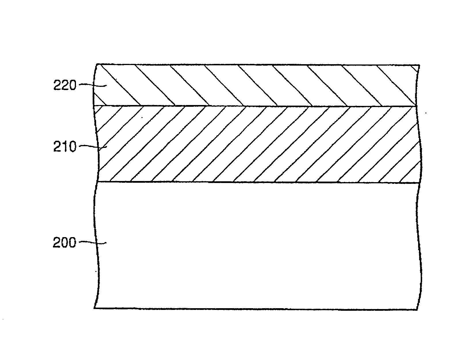
The present invention provides an infrared laser optical element, in which a dense optical thin film with a low laser absorption and high moisture resistance is formed on the surface thereof, and a manufacturing method for the same. In this infrared laser optical element, the main surface of the optical substrate is smoothed, a BaF2 film formed on said main surface thereof and then a ZnSe film formed on said BaF2 film. The smoothing treatment for the main surface of the optical substrate is carried out by irradiating Xe gas ion beams. The BaF2 and the ZnSe films formed on said BaF2 film are formed on the main surface of the optical substrate, which has been smoothed, by Xe gas ion assisted vapor deposition. Superior performance can be achieved if the series of treatments are carried out under the specified conditions.
Description
[0001] 1. Field of the Invention[0002] The present invention generally relates to an infrared laser optical element and a manufacturing method therefor. And more specifically, it relates to an optical coated element such as a focusing lens, window, or the like to be used for an infrared laser applied to machining processes such as a high-power carbon dioxide (CO) laser, and a manufacturing method therefor.[0003] 2. Description of the Related Art[0004] Conventionally, in a processing machine using an infrared laser such as a high-power carbon dioxide laser (emission wavelength: 10.6 .mu.m), zinc selenide (ZnSe), as being transparent to infrared rays, have been used as a substrate of optical elements for the resonator and focusing systems such as an output coupling mirror, rear mirror, focusing lens and the like. On the other hand, mirrors using silicon (Si) or copper (Cu) as the optical substrate have been used for optical elements of the reflection system.[0005] An optical thin film...
Claims
Login to View More Application Information
Patent Timeline
 IPC IPC(8): G02B1/11C23C14/02C23C14/06C23C14/22G02B1/115
CPCC23C14/022G02B1/10C23C14/0694
InventorIWAMOTO, HIROMINANBA, HIROKUNI
OwnerSUMITOMO ELECTRIC IND LTD