

Simulation method, simulation program, and semiconductor device manufacturing method each employing boundary conditions
a semiconductor device and simulation program technology, applied in stochastic cad, instruments, cad techniques, etc., can solve problems such as failure of semiconductor devices, difficult selection of proper boundary conditions for simulation, and unintended simulation results
- Summary
- Abstract
- Description
- Claims
- Application Information
AI Technical Summary
Problems solved by technology
Method used
Image

Examples
Embodiment Construction
[0019] Various embodiments of the present invention will be described with reference to the accompanying drawings. It is to be noted that the same or similar reference numerals are applied to the same or similar parts and elements throughout the drawings, and the description of the same or similar parts and elements will be omitted or simplified.
[0020] The present invention is applicable to, for example, process simulations and device simulations carried out to design a semiconductor device. A term "simulation" includes process simulation and device simulation in this specification. Also an apparatus used to carry out the process simulations and device simulations is called a simulation system in this specification.
[0021] Simulation System
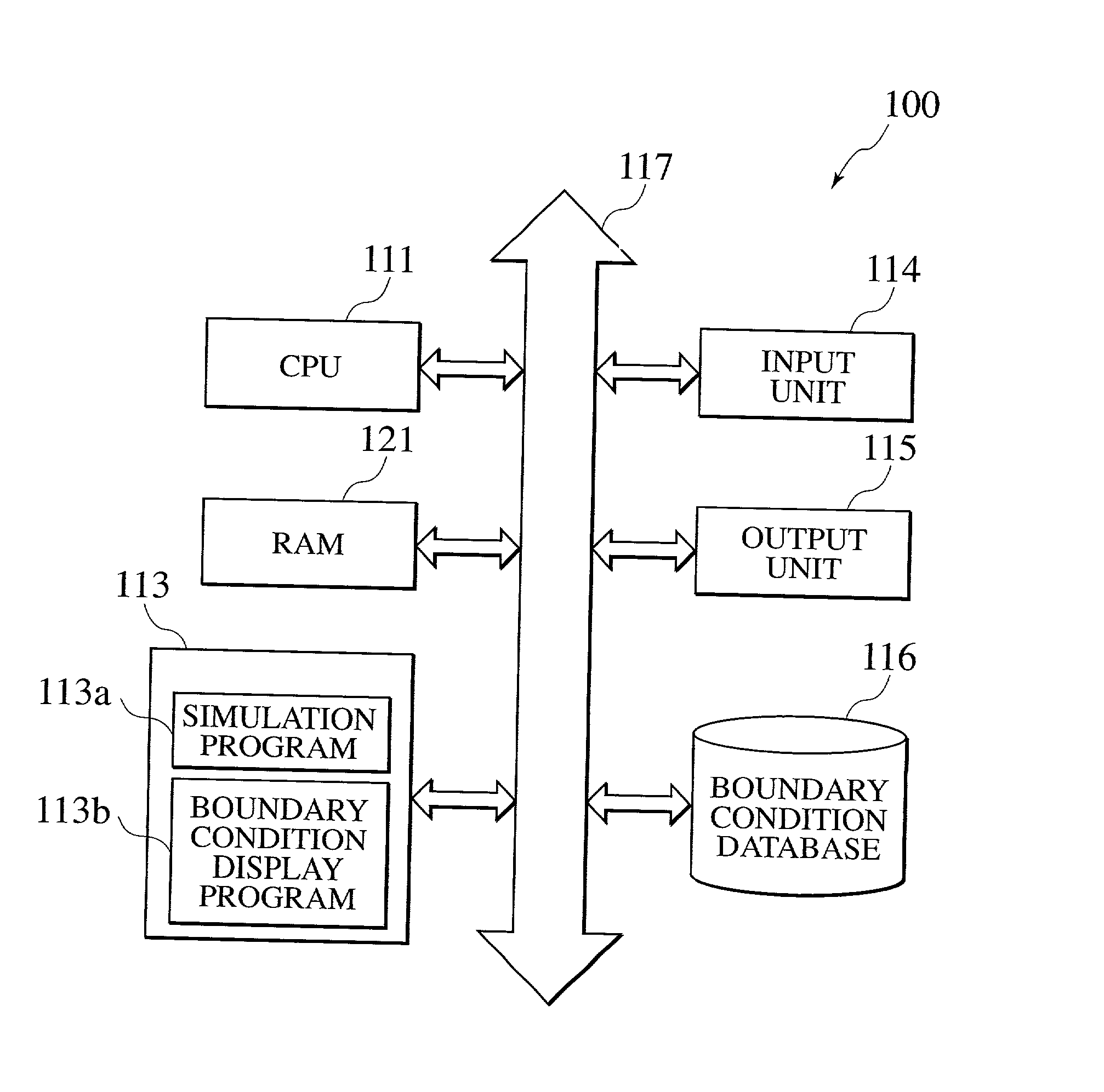
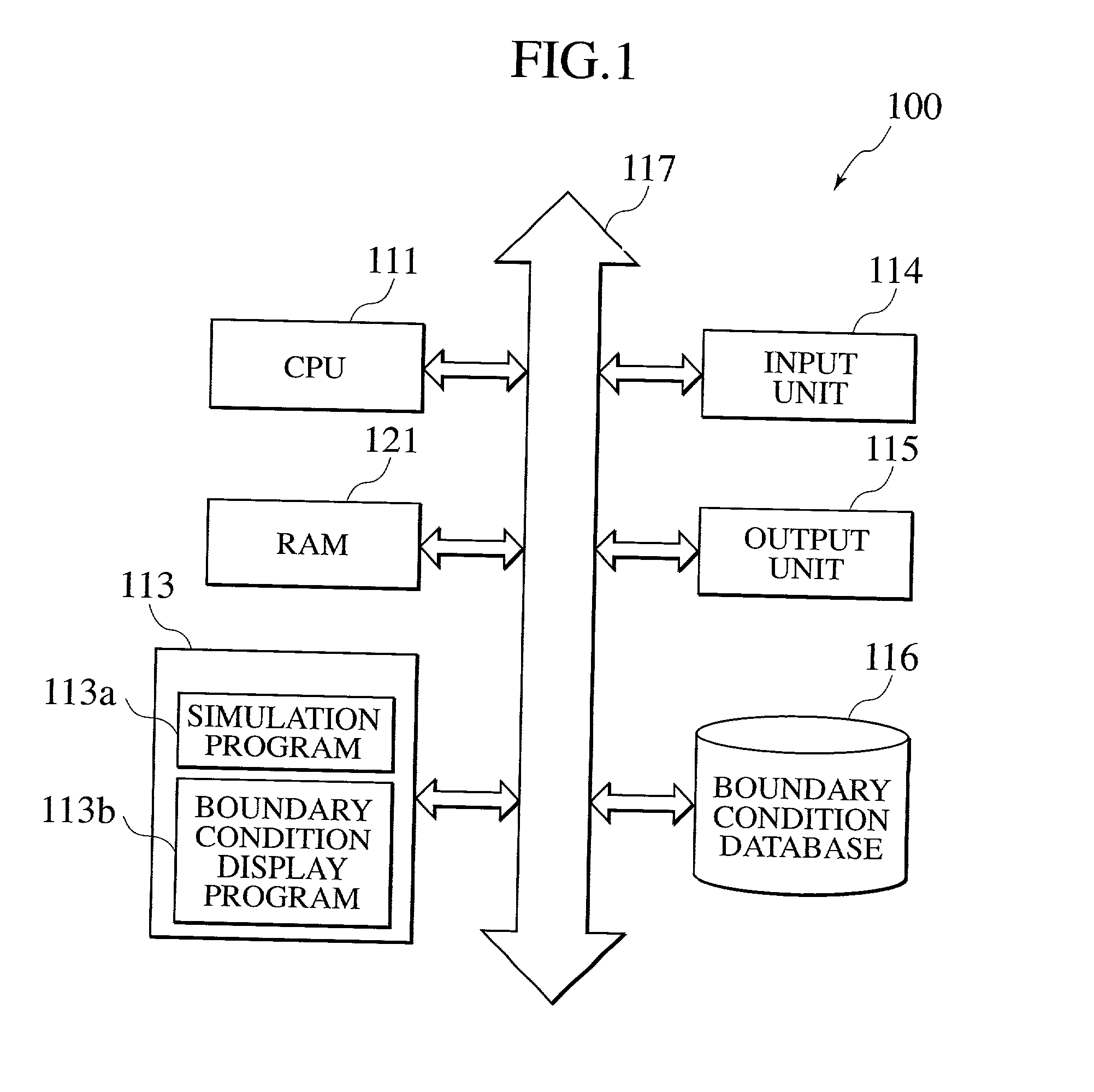
[0022] FIG. 1 is a block diagram showing a simulation system 100 according to an embodiment of the present invention. The simulation system 100 has a CPU 111, a RAM 112, a memory 113, an input unit 114, an output unit 115, a boundary condition data...
PUM
 Abstract
Description
Claims
Application Information