Systems and methods for testing bumped wafers

a technology of bumped wafers and systems, applied in the direction of electronic circuit testing, measurement devices, instruments, etc., can solve the problems of voids in solder, membrane probes are delicate and easily damaged, and need to be replaced,

Inactive Publication Date: 2002-08-08
SEMICON COMPONENTS IND LLC
View PDF0 Cites 2 Cited by
  • Summary
  • Abstract
  • Description
  • Claims
  • Application Information

AI Technical Summary

Problems solved by technology

These probes are delicate and easily damaged if there is a loose bump or a bump that includes sharp edges.
Furthermore, the membrane probe has a "tool life" and thus needs to be replaced from time to time.
However, needle probes tend to penetrate the solder which may result in voids in the solder after reflow, thus leading to a potential reliability problem.
Additiona...

Method used


Image

  • Systems and methods for testing bumped wafers
  • Systems and methods for testing bumped wafers

Examples


Embodiment Construction

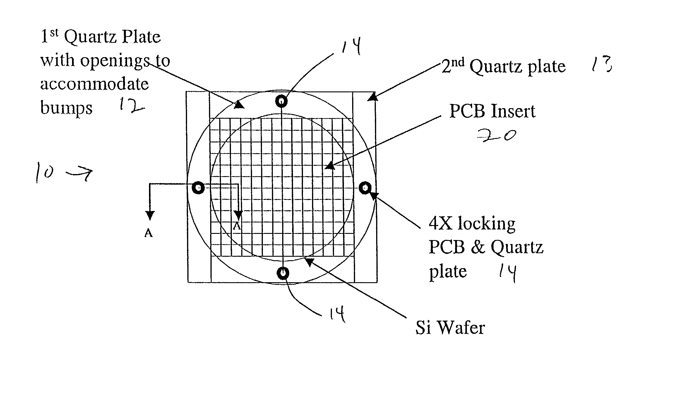
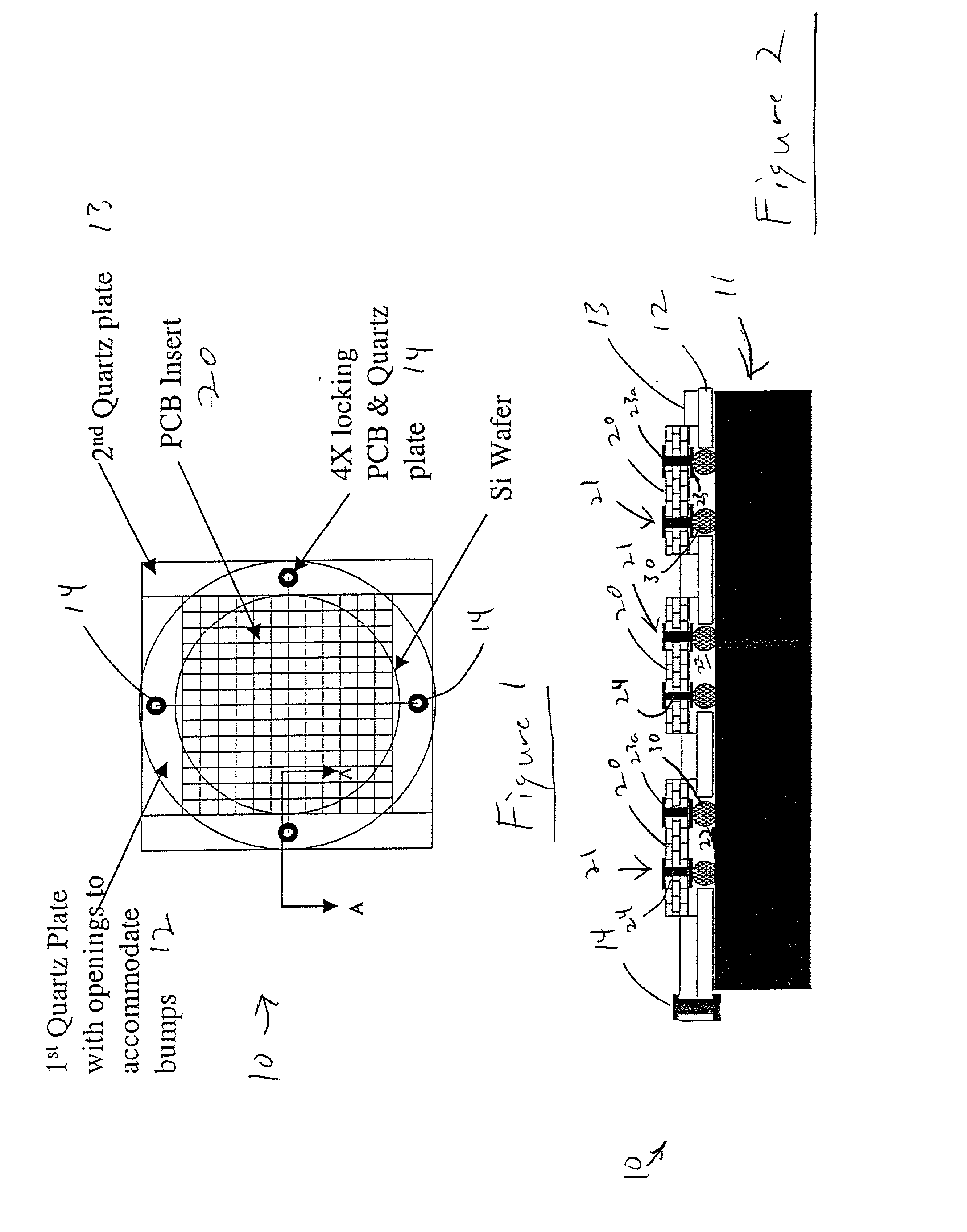
[0017] FIG. 1 illustrates a testing setup 10 for testing bumped wafers 11 according to an exemplary embodiment of the present invention. The test setup includes a first plate 12 and a second plate 13. Preferably, both plates are made of transparent material such as quartz. Examples of other types of material for the plates include glass and other solid but clear materials. The two plates are coupled to one another with coupling devices 14, preferably at four distinct locations to provide four point locking between the two plates. Examples of coupling devices include dowels, rivets, permanent glue, screws, etc. Those skilled in the art will understand that it may be possible to construct the two plates as a one-piece unit.

[0018] At least one interposer, preferably a test printed circuit board (PCB) insert, 20 is contained within the second quartz plate. Insert 20 is placed within the second quartz plate loosely such that it "floats," i.e., it is not fixedly attached to the second qua...


PUM


Abstract

A bumped wafer testing setup and associated method that eliminates the need for membrane probes. The test setup includes two plates coupled together, with the first plate including openings to accommodate solder bumps contained on the bumped wafer and the second plate including a test printed circuit board insert contained therein. The test printed circuit board insert includes solder bump contacts that contact the solder bumps within the openings.

Description

[0001] 1. Field of the Invention[0002] The present invention relates to systems and methods for testing semiconductor wafers, and more particularly, to systems and methods for testing solder bumped wafers without using membrane probes or conventional methods of probing solder bumps on the bumped wafers.[0003] 2. Description of the Prior Art[0004] A primary component of semiconductor devices is a die, which is generally aone-piece item made up of, for example, silicon. Electrical contact to a die is made by either bond wires or solder bumps. A die with solder bumps already attached is commonly referred to as a bumpted die. A bumped die generally includes the die itself, the solder bumps themselves, and an "under bump" material that serves as an intermediate layer between the top surface of the die and the solder bumps. Preferably, the under bump material is one of Tw, Cu, Au or an equivalent with one or more of the materials in layer(s). The bumped dies are generally cut from bumped ...

Claims


Application Information

Patent Timeline
IPC IPC(8): G01R31/28
CPCG01R31/2831G01R31/2886
Inventor SINGH, INDERJIT
Owner SEMICON COMPONENTS IND LLC
Why Eureka
Try Eureka