Resilient contact structures formed and then attached to a substrate

a contact structure and substrate technology, applied in the direction of printed circuit assembling, coupling device connection, non-electric welding apparatus, etc., can solve the problems of mechanical stress, inability to meet the requirements of use,

Inactive Publication Date: 2002-08-29
FORMFACTOR INC
View PDF82 Cites 363 Cited by
  • Summary
  • Abstract
  • Description
  • Claims
  • Application Information

AI Technical Summary

Benefits of technology

[0048] It is a general object of the present invention to provide improved techniques for interconnecting electronic components, especially microelectronic components.
[0049] It is another object of the present invention to provide improved techniques for mounting contact structures to electronic components, especially semiconductor dies.
[0050] It is another object of the present invention to provide improved techniques for fabricating resilient contact structures.

Problems solved by technology

Preferably, such a "hermetic" coating would not be conductive, as it would tend to short out the device (die).
Surface mount technology solves certain problems associated with making interconnections between electronic components, but has proven itself not to be the panacea it was once envisioned to be.
The challenges to effecting reliable surface mount include forming solder bumps with controlled geometry and high aspect ratio (ration of height to width), sometimes referred to as "solder columns".
The manufacture of such test fixtures is a specialty requiring a different test fixture for each array pattern, and is consequently both expensive and time-consuming.
The difference in thermal coefficients of expansion between the die and surrounding elements (e.g., package, board, electrical connections) results in mechanical stress.
Moreover, each of the aforementioned techniques suffers from inherent limitations.
Sockets address this concern, but add (often unacceptable) cost to the overall system.
Moreover, socketing tends to exhibit inferior connection reliability, as contrasted with soldered connections.
Surface mount techniques, such as the aforementioned technique of providing the first electronic component with solder balls and providing the second electronic component with conductive pads require carefully controlled processes to effect reliably, and do not lend themselves well to disassembly (replacement of one of the electronic components).
For example, gold has a very low yield strength, a characteristic which makes it extremely counter-intuitive to employ a gold wire in (or as) a resilient contact structure.

Method used


Image

  • Resilient contact structures formed and then attached to a substrate
  • Resilient contact structures formed and then attached to a substrate
  • Resilient contact structures formed and then attached to a substrate

Examples


Embodiment Construction

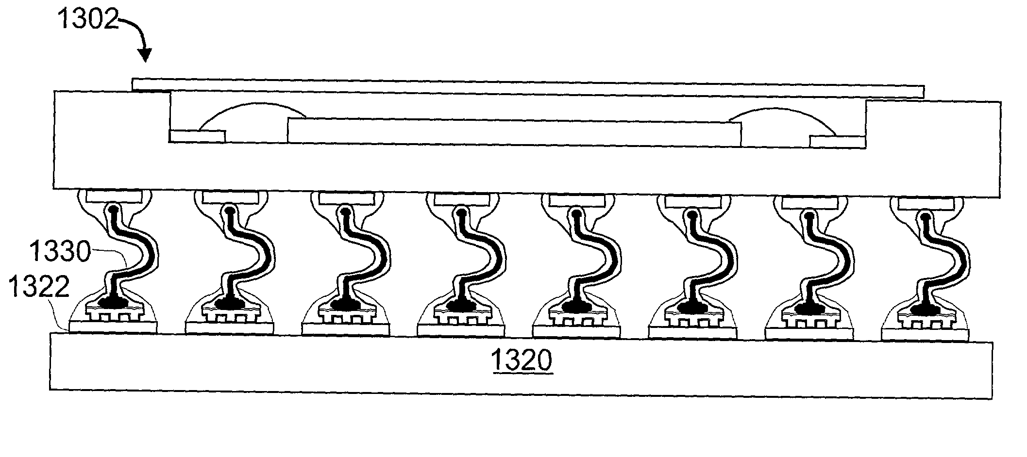
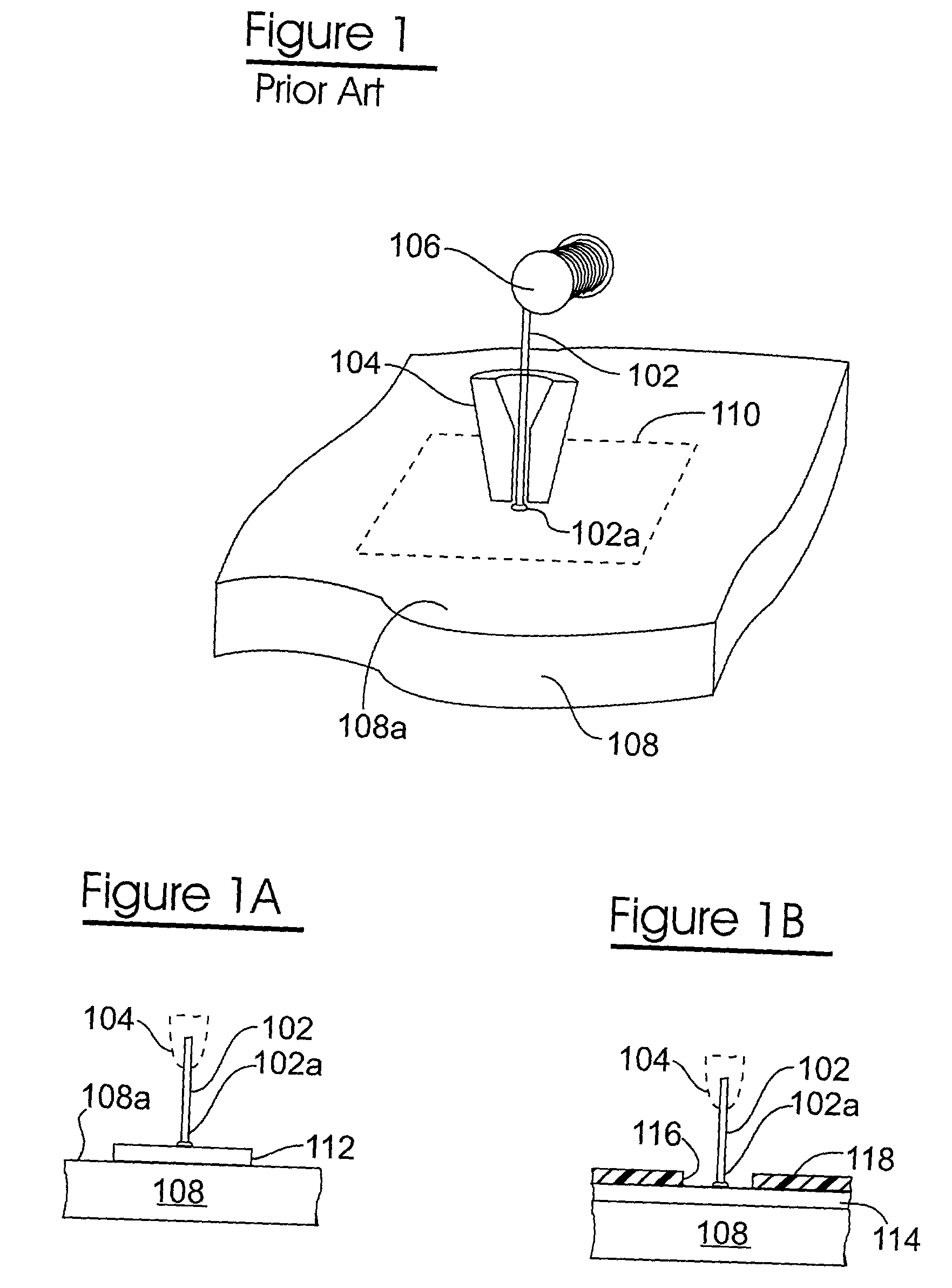
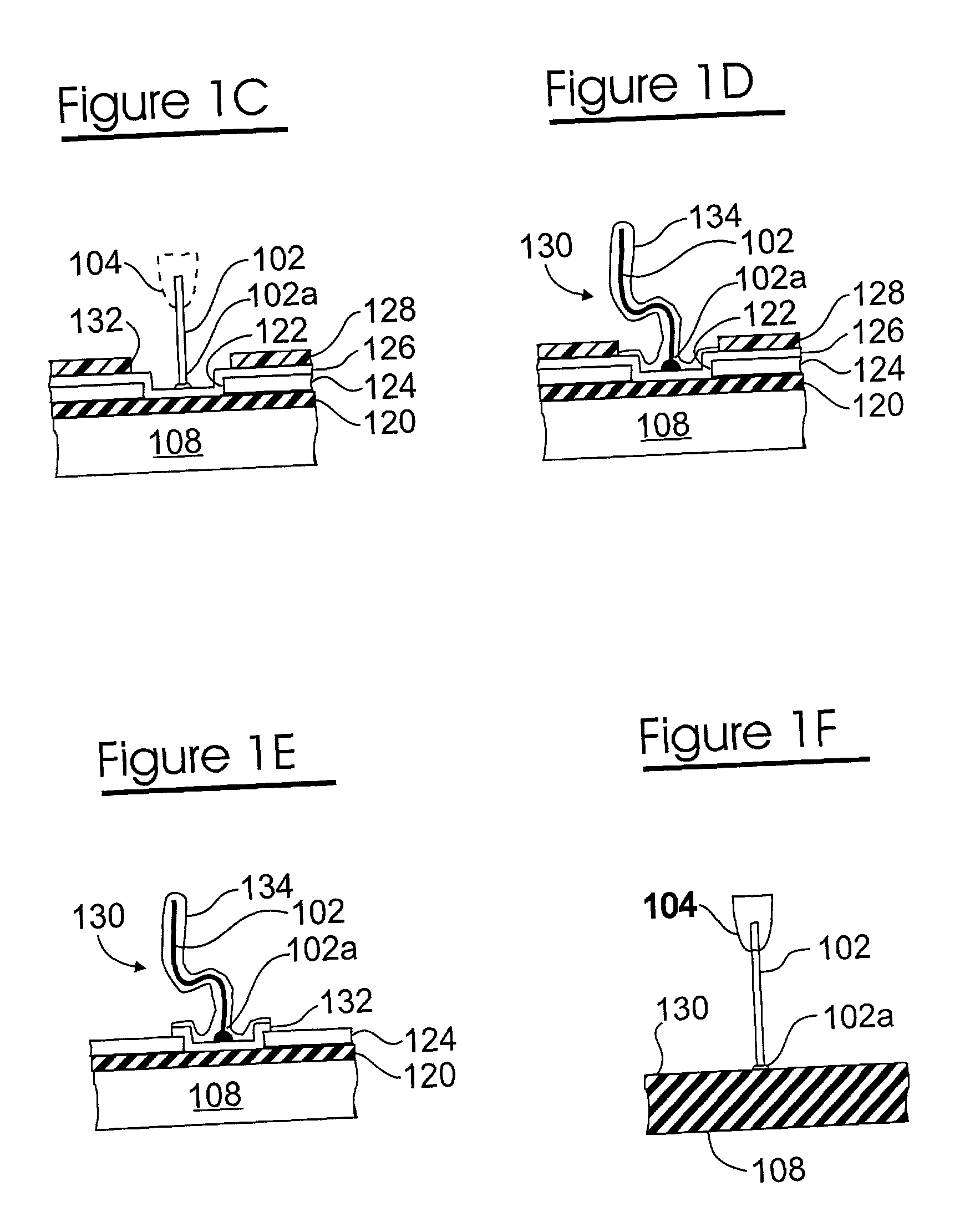
[0853] It has been described, hereinabove, how the proximal end of a wire can be bonded to a substrate, the wire configured and severed to be a freestanding wire stem having a shape suitable for overcoating to become a resilient contact structure, and overcoated to result in a freestanding contact structure having resiliency (and improved anchoring to the substrate).

[0854] It has also been mentioned (see, e.g., FIG. 2F, hereinabove) that the distal end of the wire stem can be bonded within the contact area on the substrate. Such an arrangement is particularly well adapted to overcoating the resulting loop with solder, to make solder contacts having controlled geometry and high aspect ratio, as discussed in CASE-1 and in CASE-2. These solder-overcoated loop embodiments of the invention are described only briefly, herein, since they generally fall into a category which is different than "resilient contact structures".

[0855] In many electronic applications, it is desireable to form a p...


PUM

PropertyMeasurementUnit
diameteraaaaaaaaaa
diameteraaaaaaaaaa
diameteraaaaaaaaaa

Abstract

Contact structures exhibiting resilience or compliance for a variety of electronic components are formed by bonding a free end of a wire to a substrate, configuring the wire into a wire stem having a springable shape, severing the wire stem, and overcoating the wire stem with at least one layer of a material chosen primarily for its structural (resiliency, compliance) characteristics. A variety of techniques for configuring, severing, and overcoating the wire stem are disclosed. In an exemplary embodiment, a free end of a wire stem is bonded to a contact area on a substrate, the wire stem is configured to have a springable shape, the wire stem is severed to be free-standing by an electrical discharge, and the free-standing wire stem is overcoated by plating. A variety of materials for the wire stem (which serves as a falsework) and for the overcoat (which serves as a superstructure over the falsework) are disclosed. Various techniques are described for mounting the contact structures to a variety of electronic components (e.g., semiconductor wafers and dies, semiconductor packages, interposers, interconnect substrates, etc.), and various process sequences are described. The resilient contact structures described herein are ideal for making a "temporary" (probe) connections to an electronic component such as a semiconductor die, for burn-in and functional testing. The self-same resilient contact structures can be used for subsequent permanent mounting of the electronic component, such as by soldering to a printed circuit board (PCB). An irregular topography can be created on or imparted to the tip of the contact structure to enhance its ability to interconnect resiliently with another electronic component. Among the numerous advantages of the present invention is the great facility with which the tips of a plurality of contact structures can be made to be coplanar with one another. Other techniques and embodiments, such as wherein the falsework wirestem protrudes beyond an end of the superstructure, or is melted down, and wherein multiple free-standing resilient contact structures can be fabricated from loops, are described.

Description

[0001] This is a continuation-in-part of commonly-owned, copending U.S. patent application Ser. No. 08 / 340,144, filed Nov. 15, 1994 (status pending) and its counterpart PCT patent application Ser. No. PCT / US94 / 13373, filed Nov. 16, 1994 (status pending; collectively, the US and PCT parent cases are referred to hereinafter as "CASE-2"), both of which are continuations-in-part of commonly-owned, copending U.S. patent application Ser. No. 08 / 512,812, filed Nov. 16, 1993 (status pending; referred to hereinafter as "CASE-1").[0002] The invention relates to contact structures for making electrical connections to, from and between electronic components, especially microelectronic components and, more particularly, to contact structures exhibiting resiliency and / or compliance.[0003] Due to its superior conductive and non-corrosive characteristics, gold is a "material of choice" for making electrical connections between electronic components. For example, it is well known to make a plurality...

Claims


Application Information

Patent Timeline
Patent Type & Authority Applications(United States)
IPC IPC(8): B23K20/00C23C18/16C25D5/08C25D5/22C25D7/12C25D21/02G01R1/04G01R1/067G01R1/073G01R31/28H01L21/00H01L21/48H01L21/56H01L21/60H01L21/603H01L21/66H01L23/48H01L23/485H01L23/49H01L23/498H01L25/065H01L25/16H05K1/14H05K3/20H05K3/30H05K3/32H05K3/34H05K3/36H05K3/40H05K7/10
CPCB23K20/004B23K2201/40C23C18/31C23C18/32C23C18/38C25D5/08C25D5/22C25D21/02G01R1/0483G01R1/06711G01R1/07314G01R1/07342G01R1/07357G01R1/07378G01R31/2884G01R31/2886H01L21/4853H01L21/4889H01L21/563H01L21/6715H01L21/67248H01L21/67253H01L21/67288H01L22/20H01L23/49811H01L24/11H01L24/16H01L24/45H01L24/48H01L24/72H01L24/78H01L24/81H01L24/85H01L25/0652H01L25/16H01L2224/1134H01L2224/13099H01L2224/13124H01L2224/13144H01L2224/13147H01L2224/16145H01L2224/45015H01L2224/45144H01L2224/45565H01L2224/4569H01L2224/48091H01L2224/48227H01L2224/48599H01L2224/49109H01L2224/73203H01L2224/78301H01L2224/81801H01L2224/85043H01L2224/85045H01L2224/851H01L2224/85201H01L2224/85205H01L2225/0651H01L2225/06527H01L2225/06555H01L2225/06572H01L2924/01004H01L2924/01005H01L2924/01006H01L2924/01011H01L2924/01012H01L2924/01013H01L2924/01014H01L2924/01015H01L2924/01018H01L2924/01022H01L2924/01025H01L2924/01027H01L2924/01028H01L2924/01029H01L2924/0103H01L2924/01031H01L2924/01039H01L2924/01042H01L2924/01046H01L2924/01047H01L2924/01049H01L2924/0105H01L2924/01051H01L2924/0106H01L2924/01074H01L2924/01075H01L2924/01077H01L2924/01078H01L2924/01079H01L2924/01082H01L2924/01083H01L2924/01322H01L2924/014H01L2924/10329H01L2924/14H01L2924/15153H01L2924/15165H01L2924/15312H01L2924/1532H01L2924/16195H01L2924/19041H01L2924/19043H01L2924/20751H01L2924/20753H01L2924/20754H01L2924/20755H01L2924/30105H01L2924/30107H01L2924/3011H01L2924/3025H05K1/141H05K3/20H05K3/308H05K3/326H05K3/3421H05K3/3426H05K3/368H05K3/4015H05K3/4092H05K7/1069H05K2201/0397H05K2201/068H05K2201/1031H05K2201/10318H05K2201/10378H05K2201/10719H05K2201/10734H05K2201/10757H05K2201/10878H05K2201/10909H05K2201/10946H01L2924/00014H01L2924/20752H01L24/13H01L24/49H01R12/52H01L2924/00013H01L2924/01019H01L2924/01023H01L2924/01024H01L2924/01033H01L2924/01044H01L2924/01045H01L2924/01076H01L2224/45124H01L2224/45147H01L2924/00H01L2924/10253H01L2924/12041H01L2924/07802Y10T29/49213Y10T29/49149Y10T29/49147Y10T29/49174Y10T29/49204Y10T29/49208H01L2224/13082H01L2224/13647H01L2224/13655H01L2924/19107B23K2101/40H01L2924/181H01L2924/12042H01L2924/12044H01L2224/45109H01L2224/45111H01L2224/45116H01L2224/4512H01L2224/45123H01L2224/45138H01L2224/45139H01L2224/45155H01L2224/45163H01L2224/45164H01L2224/45169H01L2224/45173H01L2224/45176H01L2224/48095H01L2224/85203H01L2224/05571H01L2224/05573H01L2224/05568H01L2224/05572H01L2224/45014Y02P70/50C25D7/0607C25D5/12C25D5/16C25D5/605H01L2924/20756H01L2924/20757H01L2924/00015H01L2924/2075H01L2924/01204H01L2924/013H01L2924/01048H01L2224/48H01L2924/00012H01L2924/206
Inventor ELDRIDGE, BENJAMIN NILESGRUBE, GARY WILLIAMKHANDROS, IGOR YANMATHIEU, GAETAN L.
Owner FORMFACTOR INC
Why Eureka
Try Eureka