Parallel test board used in testing semiconductor memory devices

a test board and semiconductor technology, applied in the field of parallel test boards, can solve the problems of increasing the number of possible defect patterns, increasing the time required for testing the device, and becoming more difficult to test for every possible defect, so as to improve the reliability of the test process

Inactive Publication Date: 2002-09-12
SAMSUNG ELECTRONICS CO LTD
View PDF0 Cites 17 Cited by
  • Summary
  • Abstract
  • Description
  • Claims
  • Application Information

AI Technical Summary

Benefits of technology

The objective of this patent is to make testing for semiconductor devices more reliable by simulating how they would operate if used in real-life situations.

Problems solved by technology

The technical problem addressed in this patent text relates to detecting issues in memory devices caused by factors like temperature, voltage, and processing environments. Current methods involve conducting individual tests on separate boards and analyzing the resulting data to identify potential faults. However, there are limitations to how many tests can be conducted simultaneously without causing delays and increased costs. Additionally, the current method requires replacing or upgrading the entire motherboard to change the memory capacity, making it hard to detect early failures. There is thus a need for a new approach that allows for accurate detection of flaws in multiple memory modules quickly and efficiently.

Method used


Image

  • Parallel test board used in testing semiconductor memory devices
  • Parallel test board used in testing semiconductor memory devices
  • Parallel test board used in testing semiconductor memory devices

Examples


Embodiment Construction

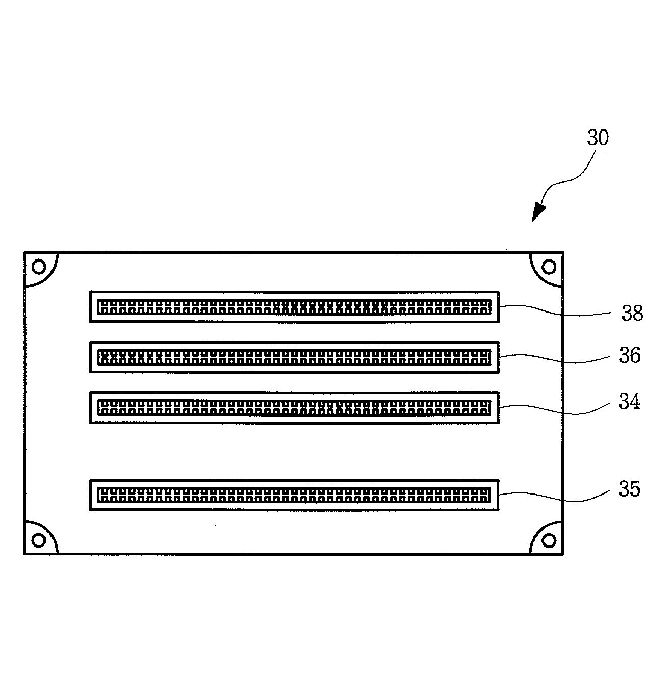
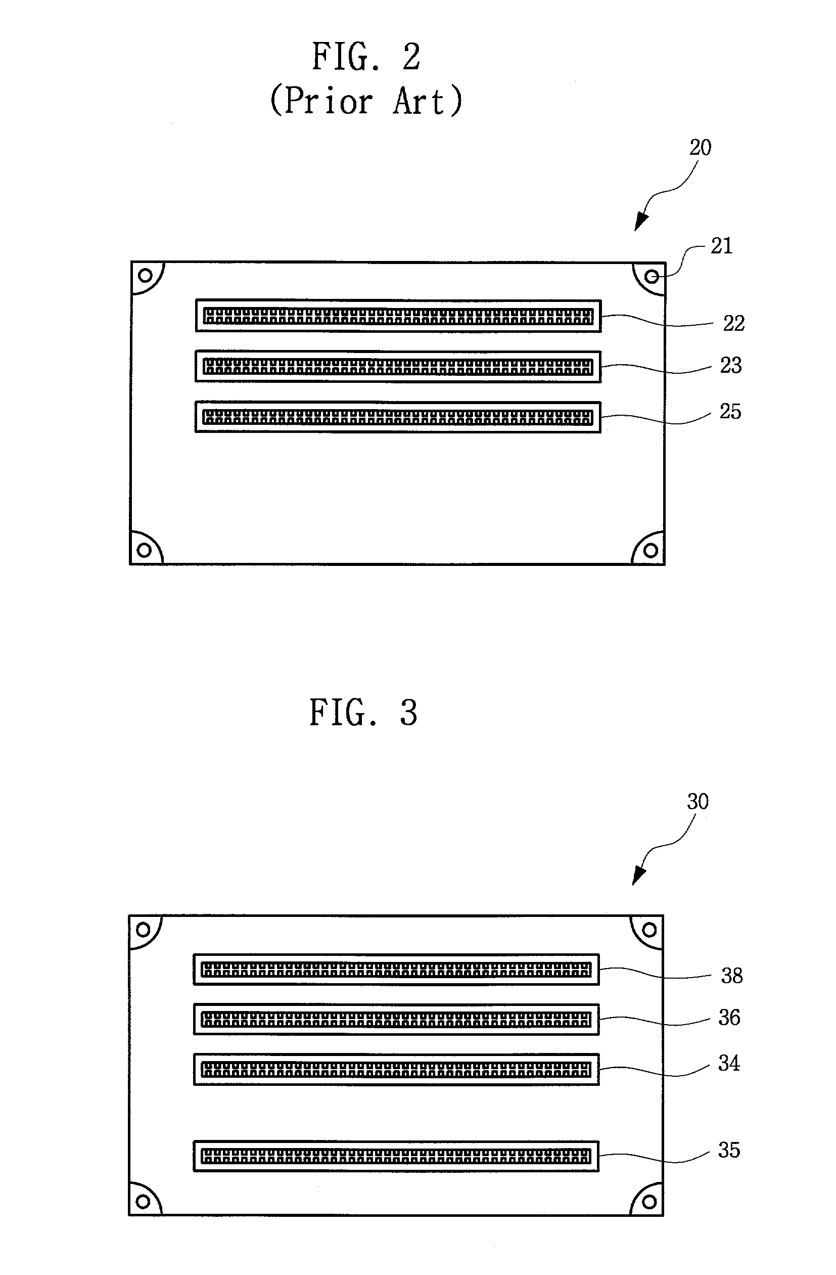
[0035] FIG. 3 is a bottom plan view of a parallel test board 30 for testing semiconductor memory devices according to one embodiment of the present invention. Referring to FIG. 3, the parallel test board 30 is provided with an extension slot 35, a reference slot 34, and a number of parallel test slots 36, 38 connected to the reference and extension slots 34, 35. Memory modules to be tested are mounted in each of the slots 34, 35, 36, 38. When the reference slot 34 operates (i.e., when read / write operations are performed to the memory module loaded in the reference slot 34), the identical read and write operations are performed to the parallel slots 36, 38. Timing distorted by the extension slot 35 affects the reference slot 34. The parallel slots 36, 38, which operate identically with the reference slot 34, are also affected.

[0036] In this manner, multi-bank operation failures, occurring when a multi-bank operation includes an external bank operation, can therefore be screened out. ...


PUM


Abstract

A parallel test board preferably includes a plurality of serial slots connected to a motherboard and a number of parallel slots connected to the motherboard in parallel with each other. The motherboard provides an actual operational environment for devices under test (DUTs). DUTs are mounted in the slots. Using a plurality of serial slots, distorted timings due to one serial slot (e.g., an extension slot) have an influence on the other serial slot (e.g., a reference slot), as well as on the parallel slots. In this manner, a timing margin failure occurring during a multi-bank operation can be effectively detected. The slots to which the DUTs are mounted preferably have a socket structure with a support block having contact pins arranged thereon. Each of the contact pins preferably has a module contact part configured to contact a tab of the DUT and a board contact part configured to contact conductive wiring patterns of an intermediation board. An elastic member is also preferably interposed between the support block and each of the module and the board contact parts. According to various aspects and embodiments of this invention, testing reliability is improved and the durability of the test board is significantly increased.

Description


Claims


Application Information

Patent Timeline
Owner SAMSUNG ELECTRONICS CO LTD
Why Eureka
Try Eureka