Probe apparatus with optical length-measuring unit and probe testing method

a technology of optical length measurement unit and probe apparatus, which is applied in the direction of measurement lead/probe, semiconductor/solid-state device testing/measurement, instruments, etc., can solve the problems of affecting the contact pressure between the probe and the chip, exposing and/or cracking the foundation layer, and excessive overdrive may damage, etc., to reduce detection errors and enhance test reliability.

Inactive Publication Date: 2005-11-17
TOKYO ELECTRON LTD
View PDF12 Cites 16 Cited by
  • Summary
  • Abstract
  • Description
  • Claims
  • Application Information

AI Technical Summary

Benefits of technology

[0007] In accordance with an aspect, the invention provides a probe apparatus capable of reducing a detection error using a simple structure, and appropriately controlling the overdrive amount to further enhance the reliability of tests, and a probe testing method for enabling such control.

Problems solved by technology

Since the foundation layers of the electrode sections or electrodes of recent chips are thin and soft, excessive overdrive may damage, expose and / or crack the foundation layers.
Accordingly, this method is disadvantageous, for example, in that the range of distances that can be measured is narrow, and the detection accuracy is low.
A detection error, if there is any, adversely influences the contact pressure between the probes and the chip.
As a result, the probes and chip may be damaged, or the probes may not satisfactorily contact the chip to cause a characteristic detection error.
Although the apparatus disclosed in this publication has two optical length-measuring units, it cannot directly detect the positions of the probes and the chip.
Therefore, much time is required for position detection, and accurate position detection cannot be achieved.

Method used


Image

  • Probe apparatus with optical length-measuring unit and probe testing method
  • Probe apparatus with optical length-measuring unit and probe testing method
  • Probe apparatus with optical length-measuring unit and probe testing method

Examples


first embodiment

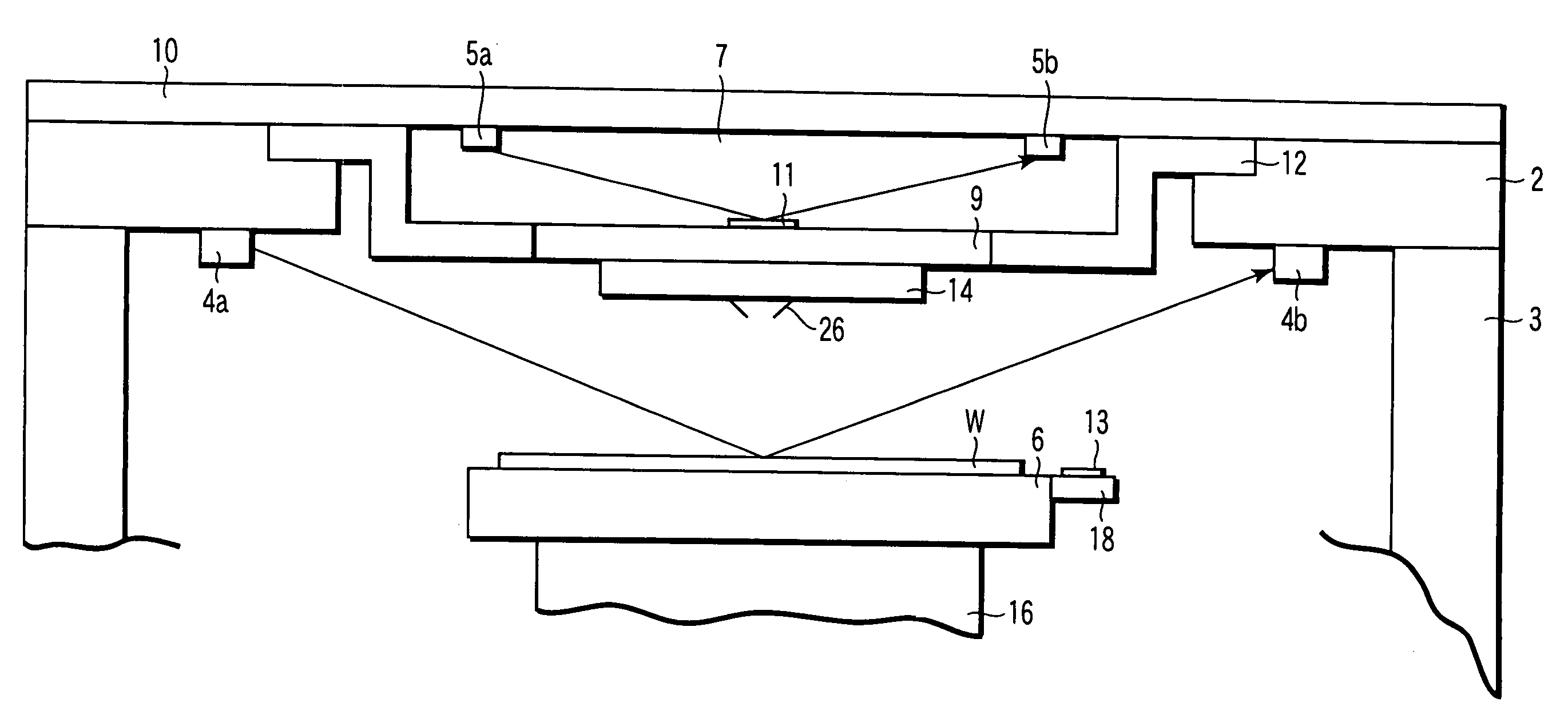
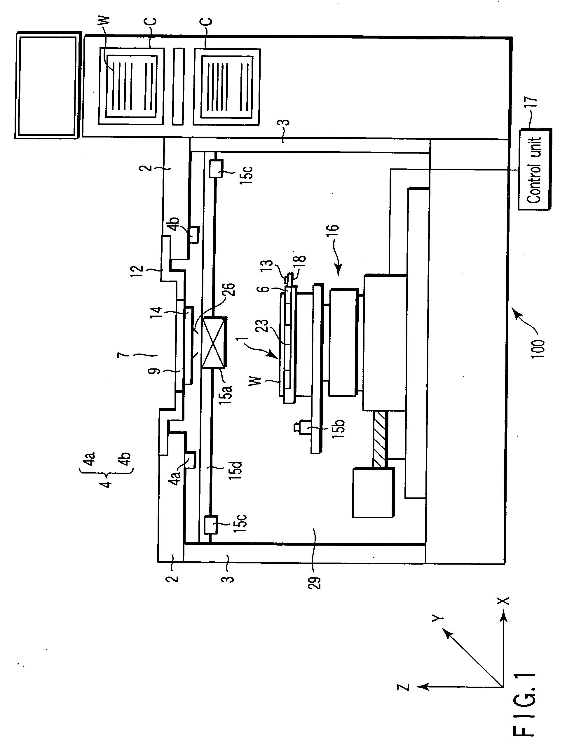
[0049] To align the Z-directional positions of each chip 1 and the probes 26, the invention employs a first optical length-measuring unit 4 (4a, 4b). The first optical length-measuring unit 4 can emit light to the surface of each chip 1 formed on the wafer W that is placed on the susceptor 6, detect the position, on a light-receiving surface thereof, of light reflected from each chip, and directly and accurately detect the Z-directional position of each chip 1 based on the detected position of light reflected. The first optical length-measuring unit 4 can be provided at any position in the prober chamber 29. However, if, in particular, it is provided on the upper wall 2 or on the upper portion of the sidewall 3, it can perform accurate position detection with little blurring.

[0050] The first optical length-measuring unit 4 includes a first irradiator 4a and first detector 4b. Light emitted from the first irradiator 4a reflects from a to-be-measured object, such as the chip 1, and en...

second embodiment

[0078] In light of the above, in the second embodiment, the second optical length-measuring unit 5 detects a change in the Z-directional position of the probe card 14. Data indicating the detected change of the probe card 14 is stored in the control unit 17. Based on the data, the control unit 17 can adjust the distance over which the susceptor 6 is raised. As a result, even if the probe card 14 is deformed during a test, the chip 1 can be brought into an appropriate contact with the probes 26. This being so, the positions of all chips 1 on the wafer W can be detected accurately and reliably.

[0079]FIG. 8 shows a third embodiment of the invention. The third embodiment is directed to a probe apparatus that comprises a second optical length-measuring unit 5 (5a, 5b), as well as the elements of the first embodiment. The second optical length-measuring unit 5 can have the same structure and function as that of the second embodiment. In the third embodiment, the second optical length-meas...


PUM


Abstract

A probe apparatus with control-position detection means is provided for testing an electrical characteristic of a to-be-tested object formed on a substrate W. The probe apparatus includes a prober chamber, a susceptor provided in the prober chamber for placing thereon a to-be-tested object, and a moving mechanism for moving the susceptor in X-, Y-, Z- and θ-directions. The probe apparatus further includes a probe card having a plurality of probes and opposing the susceptor, and a first optical length-measuring unit. The first length-measuring unit emits light to the surface of the to-be-tested object placed on the susceptor, and detects the Z-directional position of the to-be-tested object based on the light reflected from the object. The probe apparatus can have a second length-measuring unit.

Description

CROSS-REFERENCE TO RELATED APPLICATIONS [0001] This is a Continuation Application of PCT Application No. PCT / JP2004 / 000309, filed Jan. 16, 2004, which was published under PCT Article 21(2) in Japanese. [0002] This application is based upon and claims the benefit of priority from prior Japanese Patent Application No. 2003-011140, filed Jan. 20, 2003, the entire contents of which are incorporated herein by reference.BACKGROUND OF THE INVENTION [0003] 1. Field of the Invention [0004] The present invention relates to a probe apparatus and probe testing method for testing the electrical characteristic of a plurality of to-be-tested objects (hereinafter referred to as “chips”) provided on a substrate (hereinafter referred to as a “wafer”) W. More particularly, it relates to a probe apparatus that includes detection means for directly detecting the position of each chip and the position of a probe card, and a probe testing method. [0005] 2. Description of the Related Art [0006] To detect t...

Claims


Application Information

Patent Timeline
Patent Type & Authority Applications(United States)
IPC IPC(8): G01R1/06G01R31/28H01L21/66
CPCG01R31/2891G01R31/2887H01L22/00
Inventor KOMATSU, SHIGEKAZUHYAKUDOMI, TAKANORICHAYA, HIROMIHAYASHI, TAKAHISASHIGENO, YUKIHIDE
Owner TOKYO ELECTRON LTD
Why Eureka
Try Eureka