Semiconductor wafer manufacturing process

Inactive Publication Date: 2002-09-12
MEMC ELECTONIC MATERIALS INC
View PDF3 Cites 40 Cited by
  • Summary
  • Abstract
  • Description
  • Claims
  • Application Information

AI Technical Summary

Benefits of technology

0009] Among the objects of the present invention, therefore, are the provision of a process for producing a low cost semiconductor wafer having an epitaxial silicon layer; the provision of a process for growing an epitaxial silicon layer directly on an

Problems solved by technology

These defects can severely degrade the performance of circuits fabricated on the wafer, and can make the wafer unfit for grade 1 product.
Although this method does substantially eliminate many of the above-described defects, it is a slow and costly process.
This approach adds additional processing steps and requires costly equipment to implement.

Method used


Image

  • Semiconductor wafer manufacturing process
  • Semiconductor wafer manufacturing process
  • Semiconductor wafer manufacturing process

Examples


Example

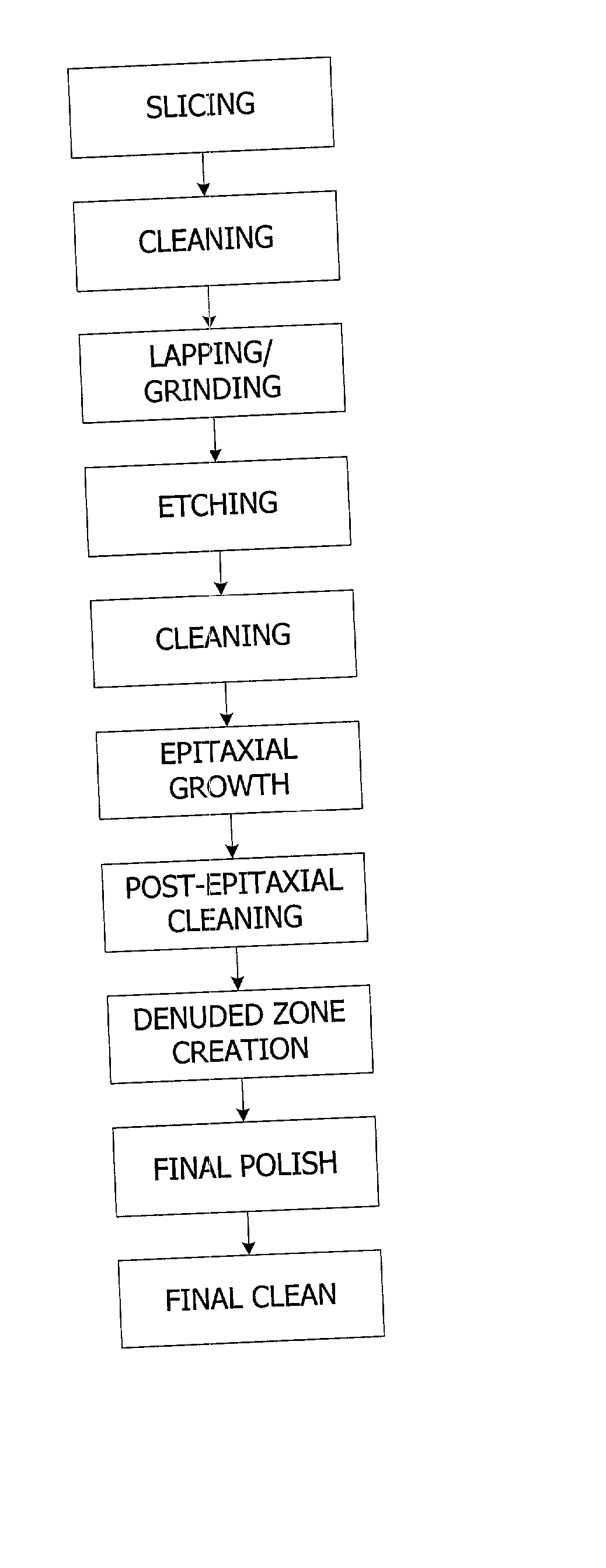
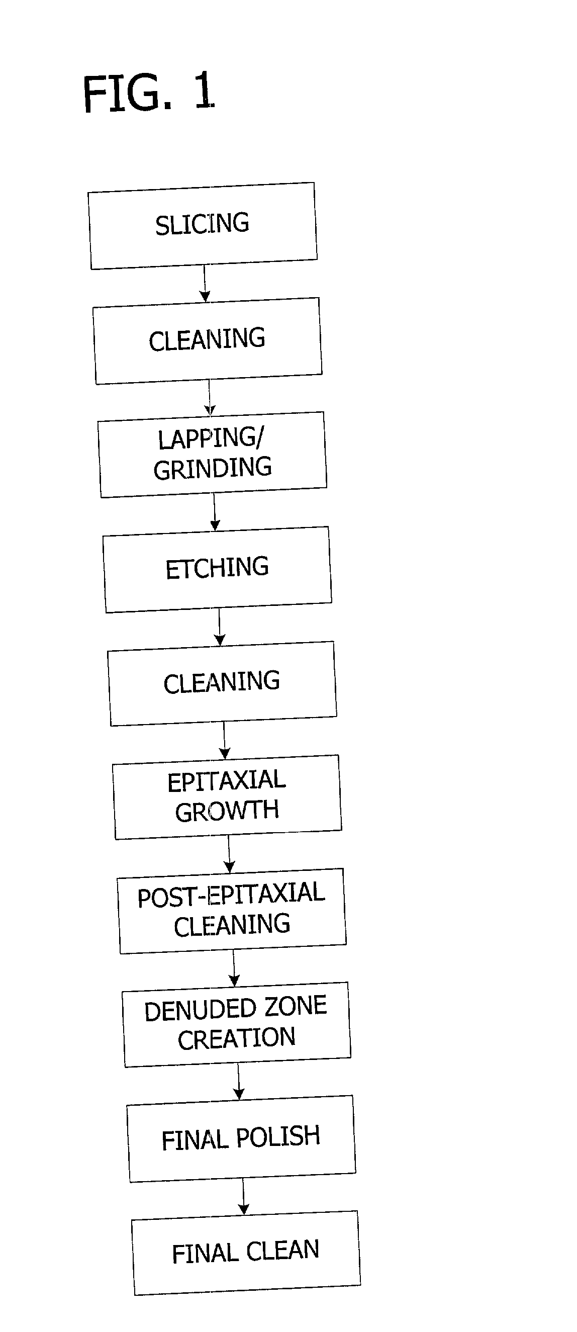
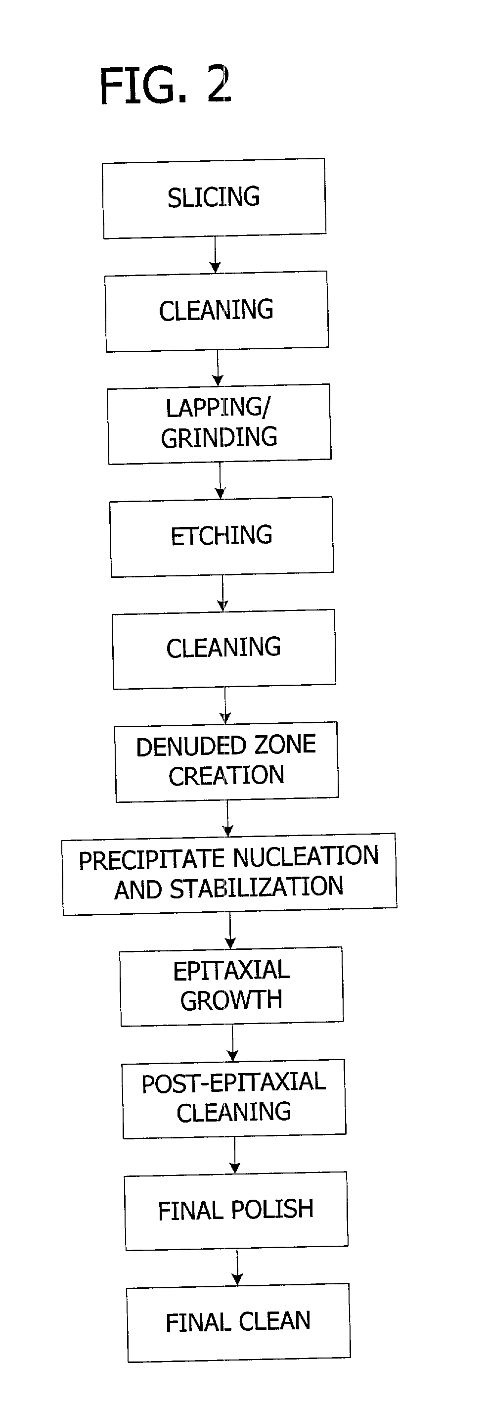
[0017] In accordance with the present invention, it has been discovered that low-cost, high quality semiconductors wafers having an epitaxial layer on the front surface can be produced in a simplified manufacturing process wherein the epitaxial silicon layer is grown directly onto an etched semiconductor surface followed by a final polish. Surprisingly, it has been shown that perturbations in the geometry of the epitaxial silicon layer due to the surface roughness of the etched surface which can interfere with patterning during device manufacturing are substantially eliminated by the final polishing. Advantageously, the semiconductor wafer of the present invention can also be subjected to a process for increasing the internal gettering capabilities of the wafer without adversely effecting the epitaxial layer.

[0018] Referring now to FIG. 1, there is shown a flow chart detailing the process steps of the present invention to produce low cost semiconductor wafers having an epitaxial lay...


PUM


Abstract

A process for manufacturing a semiconductor wafer comprises first etching the wafer to reduce damage on the front and back surfaces. An epitaxial layer is grown on the etched front surface of the semiconductor wafer to improve the surface roughness of the front surface. Finally, the front surface of the wafer is final polished to further improve the surface roughness of the front surface.

Description

CROSS-REFERENCE TO RELATED APPLICATION[0001] This application claims priority from U.S. patent application Ser. No. 60 / 258,414 (provisional), filed Dec. 27, 2000, which is hereby incorporated by reference.BACKGROUND OF THE INVENTION[0002] The present invention relates to a process for manufacturing semiconductor wafers. More particularly, the present invention relates to a simplified process for manufacturing high quality semiconductor wafers having an epitaxial silicon layer on the front surface.[0003] Single crystal silicon is the starting material for most processes for the fabrication of semiconductor electronic components and is commonly prepared with the so-called Czochralski process. In this process, a crystal pulling apparatus purged with a continuous stream of argon is utilized wherein polycrystalline silicon ("polysilicon") is charged to a quartz crucible with or without dopant, the polysilicon is melted, a seed crystal is immersed into the molten silicon and a single crys...

Claims


Application Information

Patent Timeline
IPC IPC(8): C30B23/00C30B25/00C30B28/12C30B28/14H01L21/00H01L21/20H01L21/205H01L21/302H01L21/304H01L21/322H01L23/00
CPCH01L21/02008H01L21/02532H01L21/02573H01L21/0262H01L21/3225
Inventor RIES, MICHAEL J.WILSON, GREGORY M.STANDLEY, ROBERT W.SHIVE, LARRY W.ROSSI, JON A.
Owner MEMC ELECTONIC MATERIALS INC
Why Eureka
Try Eureka