Semiconductor Memory
a technology of memory and semiconductors, applied in the field of semiconductor memory, can solve the problems of difficult to keep up with the extreme specifications of recent memory, the accuracy of testers is becoming difficult to measure the data skews involved in recent memory, and the demands of the specifications of the data output from the memory are sever
- Summary
- Abstract
- Description
- Claims
- Application Information
AI Technical Summary
Problems solved by technology
Method used
Image


Examples
first embodiment
[0023] (First Embodiment)
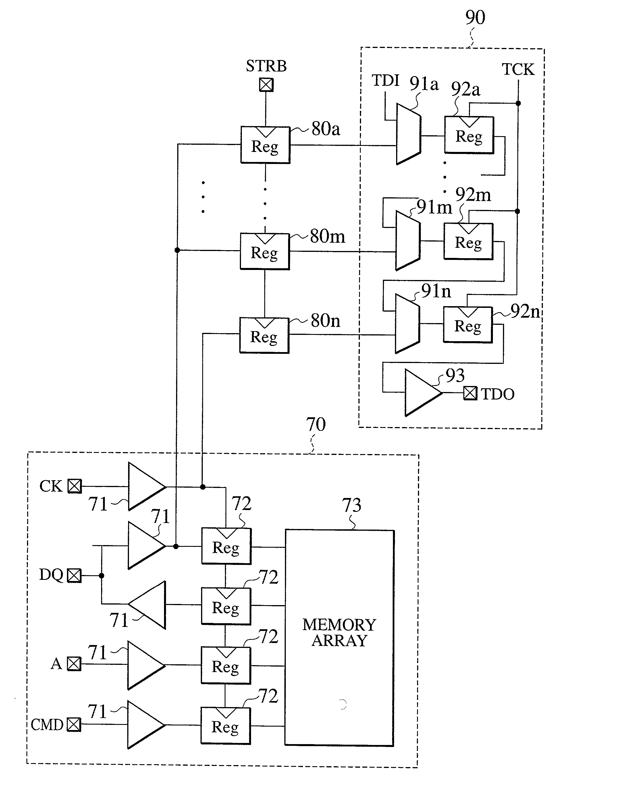
[0024] As shown in FIG. 3, the memory has a memory core 1, timing test circuit 2 (2a to 2i), and a boundary scan circuit 3. The memory core 1 includes buffers 11, registers 12, and a memory array 13. Data DQ, an address A, and a command CMD are retrieved and held in the registers 12 through the buffers 11 in synchronization with a clock signal CK. The data pieces in the registers 12 are supplied to the memory array 13. The data DQ and clock signal CK are also supplied to the timing test circuit 2. The data DQ in FIG. 3 is simply displayed. In practice, the data DQ has a data width of a plurality of bits, and all of the bits are supplied to the timing test circuit 2. If the data width of the data DQ is eight bits, the lowest bit is supplied to the timing test circuit 2a, the highest bit to the timing test circuit 2h, and the remaining bits are shared respectively by timing test circuit (not shown) between the timing test circuit 2a and 2h.
[0025] Outputs of th...
second embodiment
[0043] (Second Embodiment)
[0044] As shown in FIG. 8, the timing test circuit 2 has a register 25 (first register) to retrieve and hold input data IN in synchronization with a first strobe signal STRB1 (first timing); a register 26 (second register) to retrieve and hold input data IN in synchronization with a second strobe signal STRB2 (second timing); an exclusive OR gate 27 (logic gate) to receive the outputs of the registers 25 and 26; a delay circuit 28 to delay the second strobe signal STRB2 so as to generate a third timing; a register 29 (third register) to retrieve and hold the output of the gate 27 in synchronization with the output of the delay circuit 28; and an RS flip-flop (F / F) 30 to receive the output of the register 29. Pulse generating timing of the first and second strobe signals is the same as that in the first embodiment. In comparison with the first embodiment, the second embodiment is characterized in that both of two data pieces to be compared with each other in...
third embodiment
[0047] (Third Embodiment)
[0048] As shown in FIG. 9, the third embodiment is characterized in:
[0049] (a) a register 41 is employed to hold data in synchronization with a rising edge of a strobe signal STRB instead of the register 25 of FIG. 8;
[0050] (b) a register 42 is employed to hold data in synchronization with a falling edge of the strobe signal STRB instead of the register 26 of FIG. 8;
[0051] (c) a delay circuit 43 is employed to delay the strobe signal STRB instead of the delay circuit 28 of FIG. 8; and
[0052] (d) a register 44 is employed to hold data in synchronization with a falling edge of the output of the delay circuit 43, i.e., the register 44, instead of the register 29 of FIG. 8.
[0053] Compared with the second embodiment, the third embodiment is characterized in that a rising edge of the strobe signal STRB functions like the first strobe signal STRB1 of the second embodiment, and a falling edge of the strobe signal STRB functions like the second strobe signal STRB2 of ...
PUM
 Abstract
Description
Claims
Application Information
 - R&D
- Intellectual Property
- Life Sciences
- Materials
- Tech Scout
- Unparalleled Data Quality
- Higher Quality Content
- 60% Fewer Hallucinations
Browse by: Latest US Patents, China's latest patents, Technical Efficacy Thesaurus, Application Domain, Technology Topic, Popular Technical Reports.
© 2025 PatSnap. All rights reserved.Legal|Privacy policy|Modern Slavery Act Transparency Statement|Sitemap|About US| Contact US: help@patsnap.com