
System and method for compensation of active element variations in an active-matrix organic light-emitting diode (OLED) flat-panel display

a technology of organic light-emitting diodes and active elements, which is applied in the field of system and method of providing brightness uniformity in the active matrix oled flat-panel display, can solve the problems of display subject to more serious threshold non-uniformities, current non-uniformities between pixels, and non-uniform brightness

Active Publication Date: 2006-04-27
ADVANTECH GLOBAL LTD
View PDF10 Cites 43 Cited by
  • Summary
  • Abstract
  • Description
  • Claims
  • Application Information

AI Technical Summary

Benefits of technology

[0010] The present invention is a brightness compensation system and method for providing brightness uniformity in an active-matrix OLED flat-panel display. The present invention anticipates the use of control and memory circuits built into the interface circuitry of an active-matrix display that uses a current-dependent, light-emitting medium to completely compensate for inconsistencies in the threshold voltage and gain of the active elements (thin film transistors), both in the display and in the peripheral row and column addressing circuits. Because the measurement and corrective functions are built into the display interface circuitry, the corrective sequence, which may last as little as a few seconds, can be activated at any time, as required. For example, the corrective sequence may be automatically activated every time the display power is cycled; or, alternatively, the corrective sequence may be automatically activated on any desired time interval, such as weekly, daily, or hourly. In this way, the present invention assures that each display element delivers the exact current at its output that is required by the brightness signal of the video input signal.

Problems solved by technology

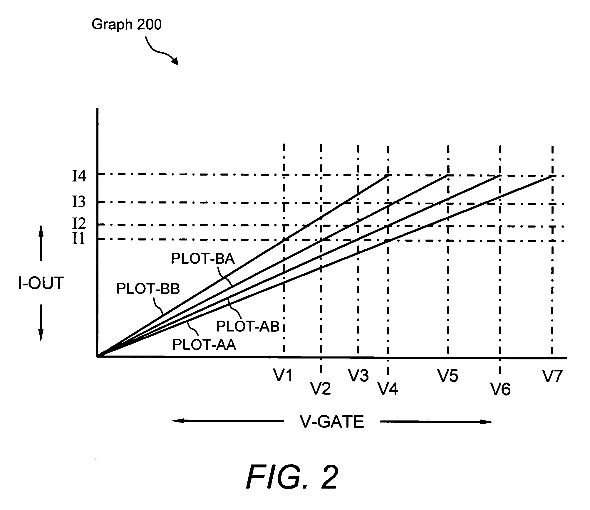
Threshold voltage variation in such a TFT, which may be caused by variations in the manufacturing process, leads to current non-uniformities between pixels and non-uniform brightness.
However, in a large-screen display application, such as a flat-panel television, the display undergoes more serious threshold non-uniformities, and the quality of the display, such as brightness uniformity, is noticeably degraded.
Therefore, there is a technical challenge in ensuring that the power transistors that drive the OLEDs are uniform and, secondly, if they are not uniform, there is a technical challenge in correcting the non-uniformity.
While the '661 patent describes a suitable method of providing compensation, it does so by using a complex process of capturing images of each pixel with a camera system.

Method used


Image

  • System and method for compensation of active element variations in an active-matrix organic light-emitting diode (OLED) flat-panel display
  • System and method for compensation of active element variations in an active-matrix organic light-emitting diode (OLED) flat-panel display
  • System and method for compensation of active element variations in an active-matrix organic light-emitting diode (OLED) flat-panel display

Examples


first embodiment

[0028]FIG. 3 illustrates a functional block diagram of a brightness compensation system 300 for providing brightness uniformity within an active-matrix OLED flat-panel display in accordance with the invention. Brightness compensation system 300 is built into the display interface circuitry of an active-matrix display 305, which is representative of a typical active-matrix OLED display under test. Brightness compensation system 300 includes a system controller 310, a timing generator 312, a test brightness generator 314, a pixel address generator 316, a video formatter 318, a multiplexer (MPX) 320, an MPX 322, a memory 324, a pixel adjust device 326, a level shifter and driver 328, a current sensor 330, an analog-to-digital (A / D) converter 332, and a DC power supply (P / S) 334.

[0029] System controller 310 is representative of a standard microprocessor device, such as a Philips 8051 8-bit microcontroller or a Motorola 6816 16-bit microcontroller. Alternatively, system controller 310 is...

second embodiment

[0059]FIG. 5 illustrates a functional block diagram of a brightness compensation system 500 for providing brightness uniformity within an active-matrix OLED flat-panel display in accordance with the invention. Brightness compensation system 500 illustrates a minimal set of additions to brightness compensation system 300 of FIG. 3, in order to accomplish “n-at-a-time” element or cell measurements.

[0060] More specifically, as compared with brightness compensation system 300 of FIG. 3, the time required to measure the corrections necessary to provide brightness uniformity to all of the active matrix elements (cells) of active-matrix display 305 are reduced by a factor “n”, where “n” is the number of elemental columns being tested in parallel, a cell at a time. This is generally accomplished by including “n” current sensors, “n” A / D converters, multiplexing switches to select the group of “n” POWER BUSES, and a data signal source programmed to provide the proper test signal to the selec...


PUM


Abstract

A brightness compensation system and method of providing brightness uniformity in an active-matrix organic light-emitting diode (OLED) flat-panel display. The brightness compensation system of the present invention includes a system controller, a timing generator, a test brightness generator, a pixel address generator, a video formatter, a first and second multiplexer, a memory device, a pixel adjust device, a level shifter and driver, a current sensor, an analog-to-digital converter, a DC power supply, and an active-matrix OLED display under test. The brightness compensation system and method of the present invention subjects an active-matrix OLED display to a testing operation that alternately tests every pixel, detects its output current, which is an indicator of light output level, for a given input voltage, saves the output current value in memory, then applies a corrective voltage to each pixel, so that each pixel has the same light output (output current) as its neighboring pixel.

Description

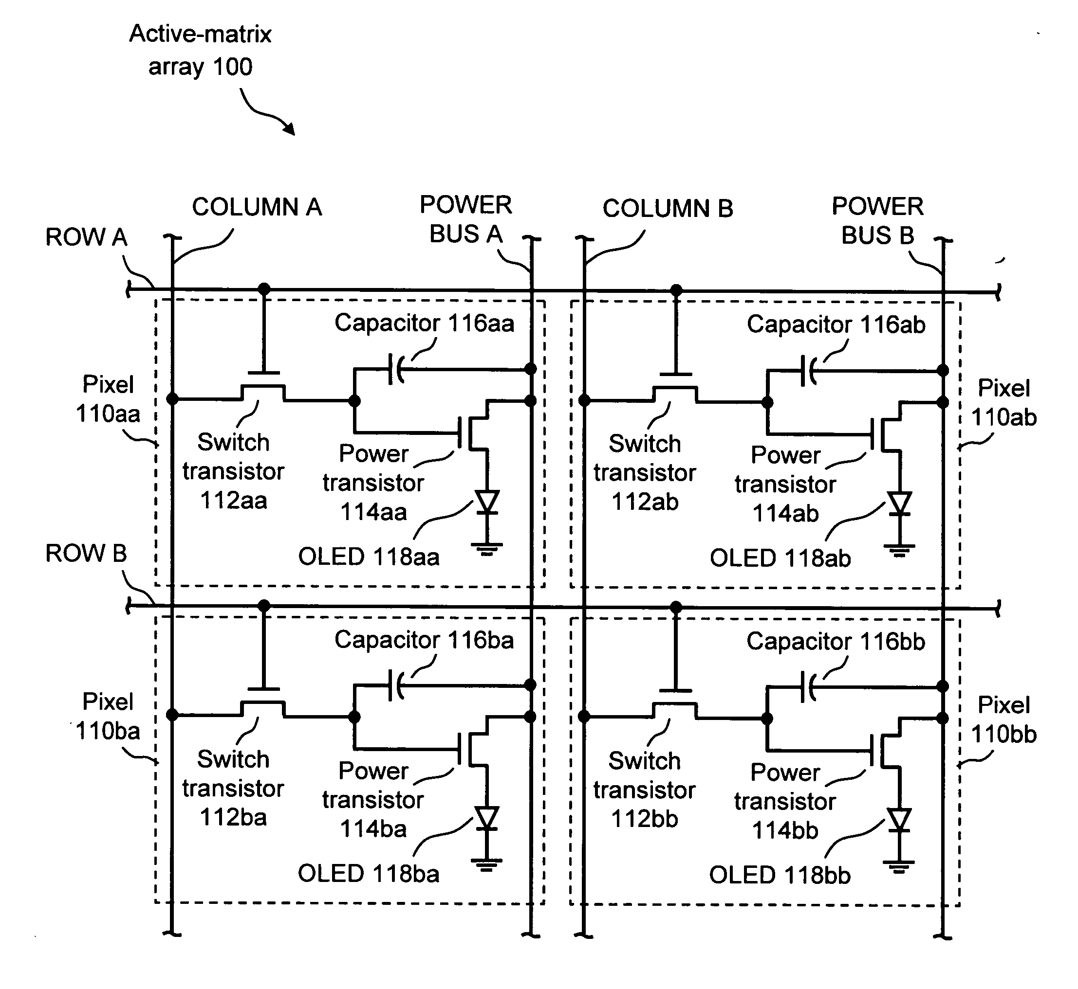
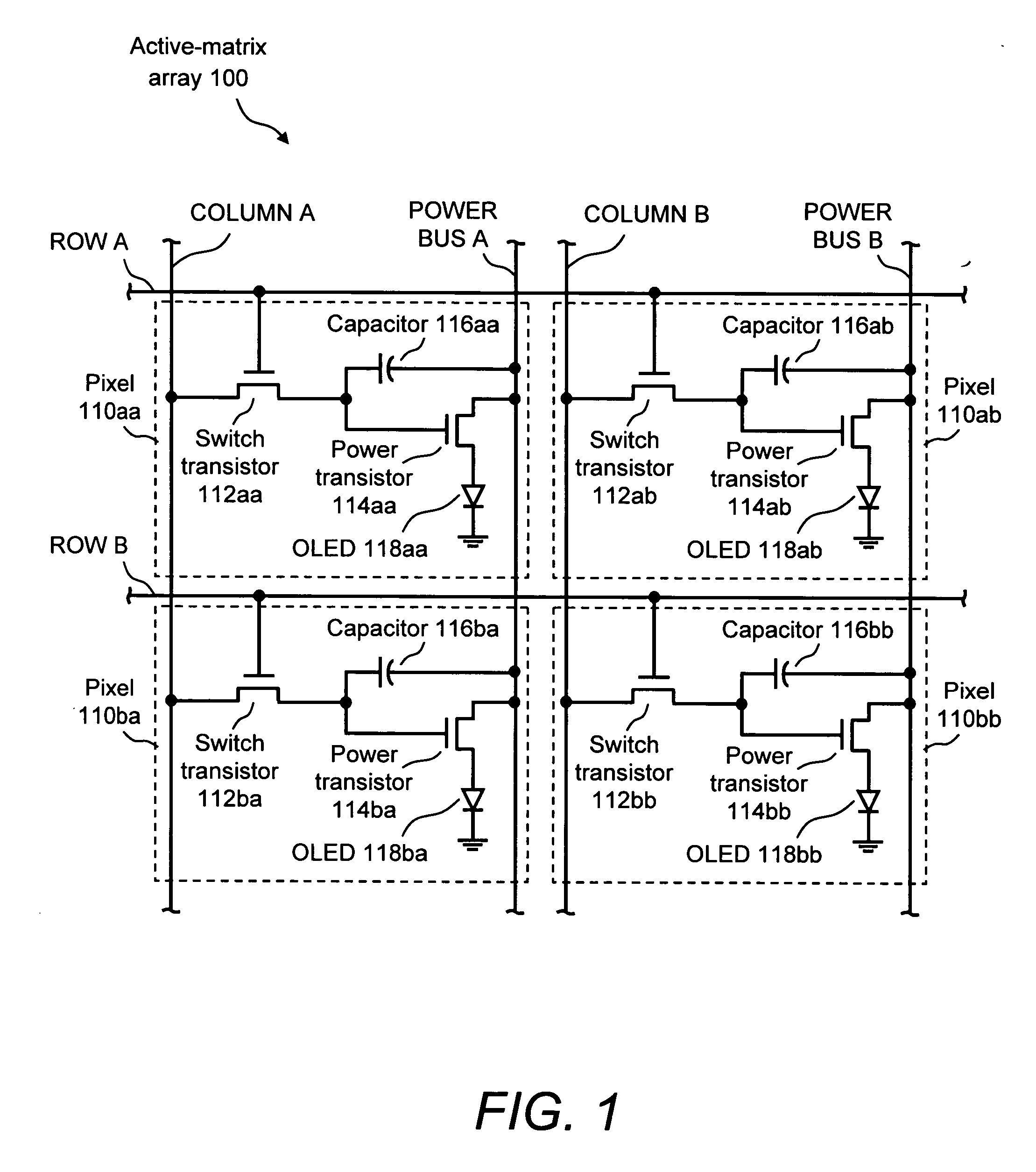
FIELD OF THE INVENTION [0001] The present invention relates to an organic light-emitting diode (OLED) flat-panel display. In particular, this invention relates to a system for and method of providing brightness uniformity in an active-matrix OLED flat-panel display. BACKGROUND OF THE INVENTION [0002] The circuit structure of an active-matrix OLED display, in which a plurality of pixels are arranged in rows and columns, is widely known. Each pixel includes two thin film transistors (TFTs), i.e., an addressing (or switching) transistor and a driving (or power) transistor, a storage capacitor, and an OLED device. [0003] As is well known, in the conventional active-matrix OLED panel circuit, a scan line (row line) is selected, a video signal loaded in a data line (column line) is input to the driving transistor via the addressing transistor to control the current through the OLED device. The video signal is stored in the storage capacitor for the duration of one frame. [0004] TFTs used ...

Claims


Application Information

Patent Timeline
Patent Type & Authority Applications(United States)
IPC IPC(8): G09G3/14
CPCG09G3/006G09G3/3258G09G2300/0809G09G2300/0838G09G2320/0233G09G2320/0285
Inventor MALMBERG, PAUL R.
Owner ADVANTECH GLOBAL LTD
Learn More