
Eureka
For R&D, Eureka makes reading and utilizing patents & technical documents easy.
Eureka AIR
Designed for self-driven R&D workflows. Generate viable solutions, solve complex R&D challenges, empower your innovation with AI.

Eureka Materials
Designed for material experts only. Revolutionize your material R&D, from search, analyze, to developing new materials.

TechResearch
Generate reliable direction feasibility study reports for your R&D in just a few steps.

TechSeek
Discover and master advanced knowledge NOW. Basics, ideas, possibilities, all at once.

TechMind
As an expert in R&D Theories, TechMind can generates customized viable solutions instantly.

TechRisk
Analyze your overall solution with one click, know your potential R&D risks in advance.

TechMonitor
Get weekly tech updates, stay abreast of the latest tech innovations and key insights.
Structure of a multi chip module having stacked chips
- Summary
- Abstract
- Description
- Claims
- Application Information
AI Technical Summary
Problems solved by technology
Method used
Image

Examples
Embodiment Construction
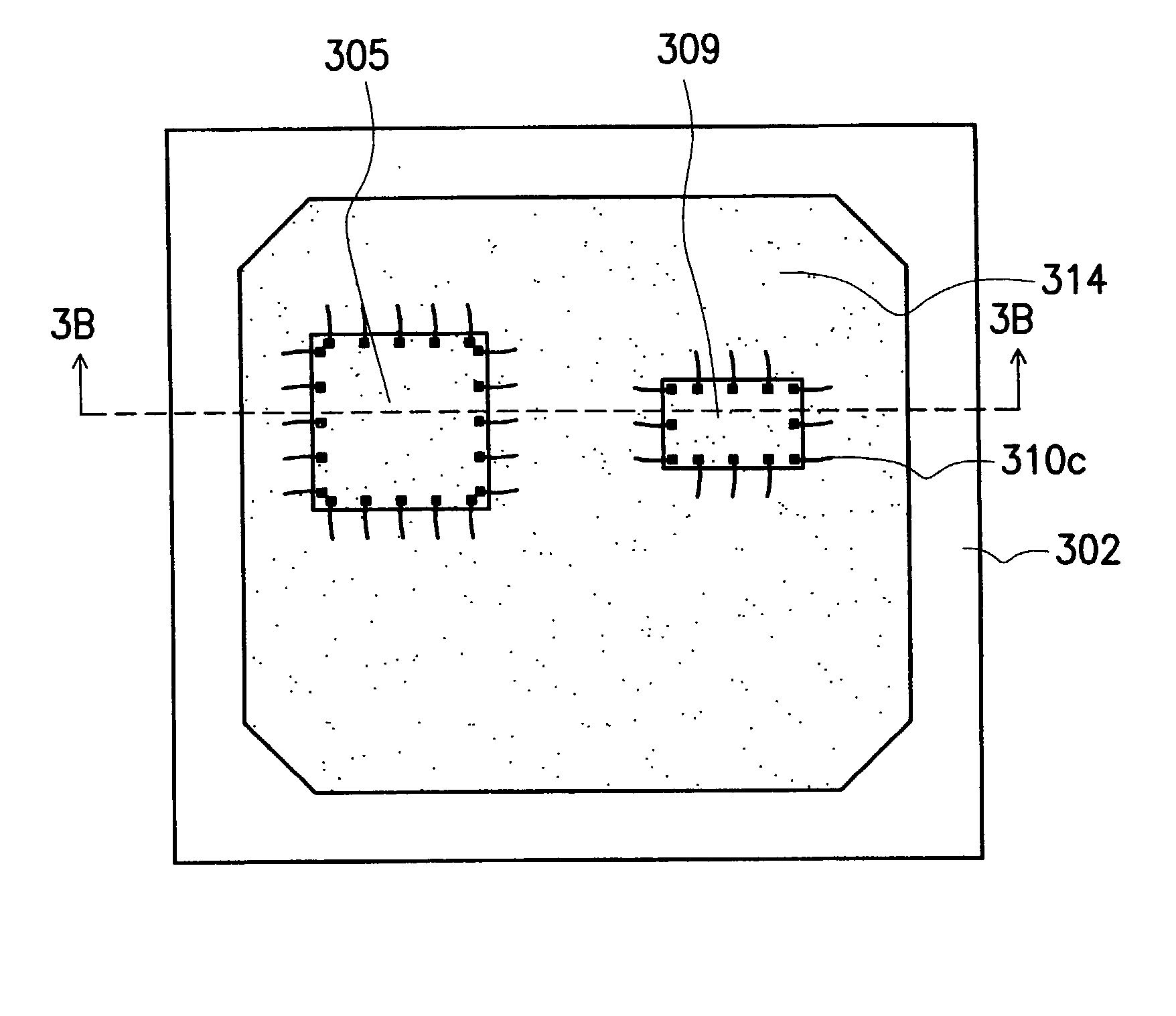
[0030] Referring to FIGS. 3A 3B, a plan view of a structure of multi chip module package having stacked chips according to the first preferred embodiments of the present invention are shown. FIG. 3B is a cross sectional view of FIG. 3A along 3B-3B.
[0031] As shown in FIGS. 3A and 3B, a substrate 302 has a front surface 301 and a back surface 303 opposite to the front surface 301. A first chip 306, a second chip 308, and a third chip 309, such as memory chips, are provided with substantially the same size. First, a main chip 305, such as a graphic chip, and the first chip 306 are provided on the front surface 301 of the substrate 302, all of which are electrically connected to the substrate 302 by wires 310a, respectively. Then, the second chip 308 is stacked on the first chip 306 and a spacer 320a. The second chip 308 is electrically connected to the substrate 302 by wires 310b. Provided on the second chip 308 is a spacer 320b. On the first chip 306, the second chip 308 and the space...
PUM
 Abstract
Description
Claims
Application Information
 - R&D Engineer
- R&D Manager
- IP Professional
- Industry Leading Data Capabilities
- Powerful AI technology
- Patent DNA Extraction
Browse by: Latest US Patents, China's latest patents, Technical Efficacy Thesaurus, Application Domain, Technology Topic, Popular Technical Reports.
© 2024 PatSnap. All rights reserved.Legal|Privacy policy|Modern Slavery Act Transparency Statement|Sitemap|About US| Contact US: help@patsnap.com