

Integration of ALD tantalum nitride and alpha-phase tantalum for copper metallization application
a technology of ald tantalum and alpha-phase tantalum, which is applied in the direction of coatings, special surfaces, chemical vapor deposition coatings, etc., can solve the problems of increasing the overall resistance, and reducing the reliability of the overall circui
- Summary
- Abstract
- Description
- Claims
- Application Information
AI Technical Summary
Problems solved by technology
Method used
Image

Examples
Embodiment Construction
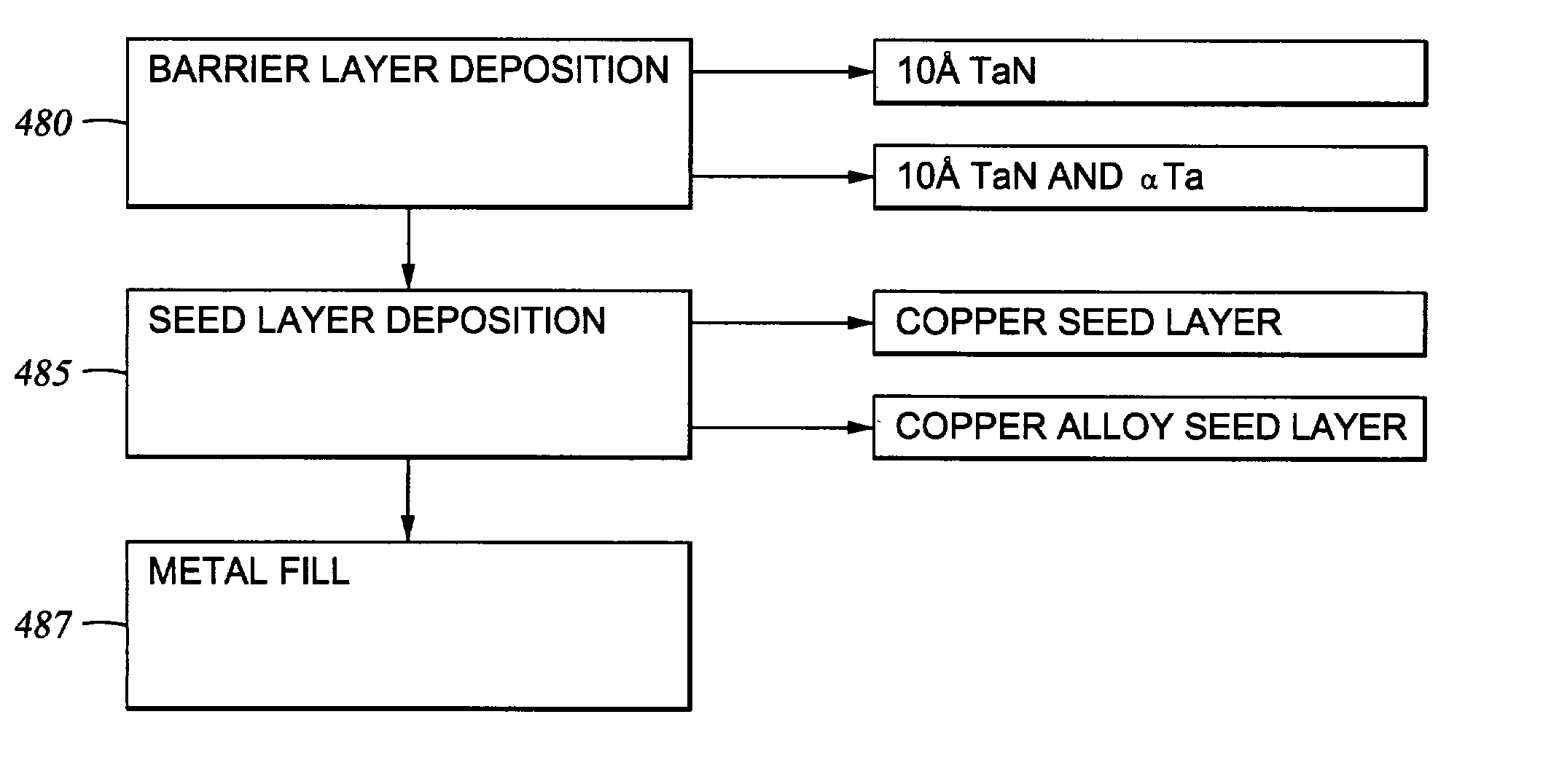
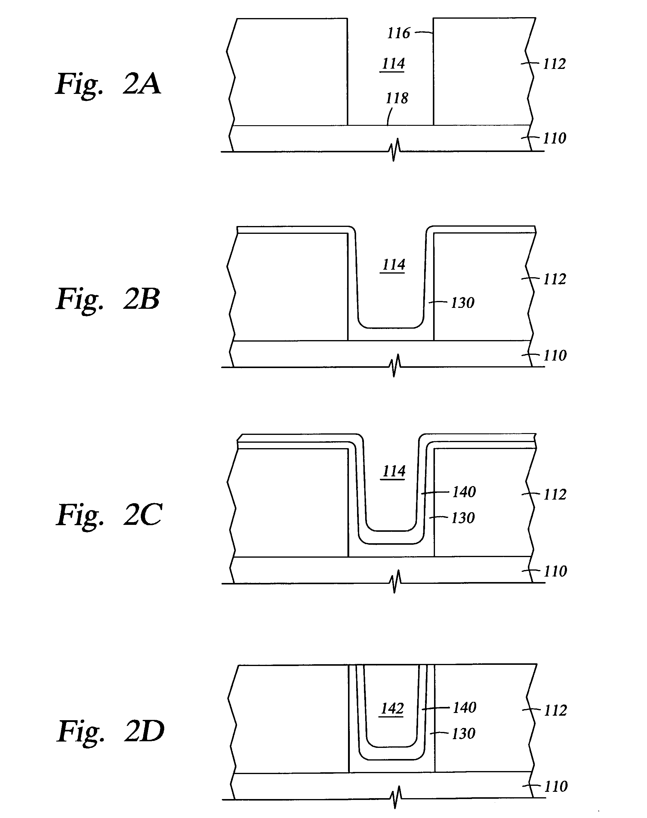
[0072] A TaN layer was deposited over a lower level copper layer using cyclical deposition to a thickness of about 20 .ANG.. A copper alloy seed layer was deposited over the TaN layer by physical vapor deposition to a thickness of about 100 .ANG.. The copper alloy seed layer contained aluminum in a concentration of about 2.0 atomic percent, and was deposited by PVD using a copper-aluminum target consisting of aluminum in a concentration of about 2.0 atomic percent. A bulk copper layer was then deposited using ECP to fill the feature. The substrate was then annealed at a temperature of about 380.degree. C. for a time period of about 15 minutes in a nitrogen (N2) and hydrogen (H2) ambient.
[0073] The overall feature resistance was significantly reduced and the upper level copper layer surprisingly exhibited a grain growth similar to that of the lower level copper layer. The barrier performance of the TaN layer exhibited longer TTF compared with 50 .ANG. PVD Ta. Further, the TaN layer s...
PUM
| Property | Measurement | Unit |
|---|---|---|
| thickness | aaaaa | aaaaa |
| thickness | aaaaa | aaaaa |
| thickness | aaaaa | aaaaa |
Abstract
Description
Claims
Application Information