Dual robot processing system

a processing system and robot technology, applied in the field of semiconductor processing system, can solve the problems of high tool cost, unavailability of small production lines, and inability to provide single layer deposition utilizing a compact mainframe, and achieve the effect of maximizing substrate processing, reducing production costs, and reducing production costs

Inactive Publication Date: 2003-06-19
APPLIED MATERIALS INC
View PDF7 Cites 164 Cited by
  • Summary
  • Abstract
  • Description
  • Claims
  • Application Information

AI Technical Summary

Benefits of technology

0021] To facilitate understanding, identical reference numerals have been used, w

Problems solved by technology

Although conventional cluster tools are generally desirable for large scale device fabrication, these systems have floor space requirements that make them impractical for smaller scale production lines.
For example, a cluster tool configured to provide single layer deposition utilizing a compact mainframe is generally not available.
As transfer chambers known to t

Method used


Image

  • Dual robot processing system
  • Dual robot processing system
  • Dual robot processing system

Examples


Embodiment Construction

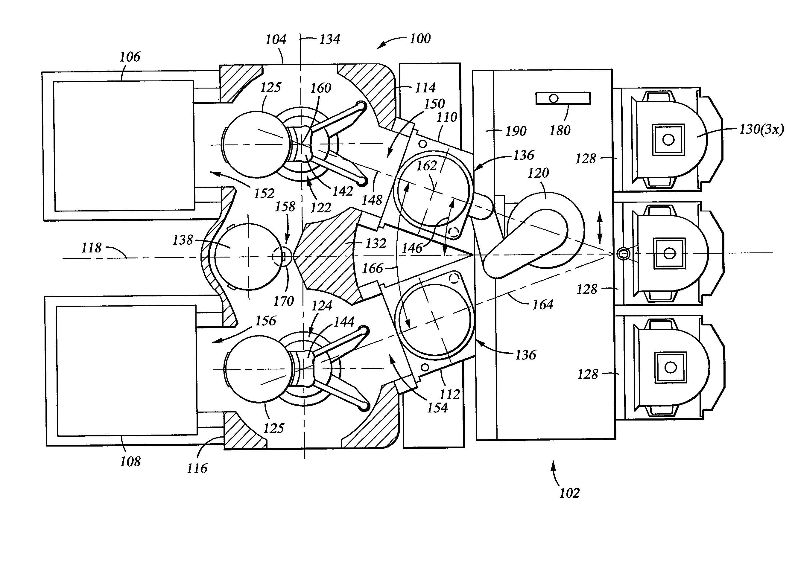
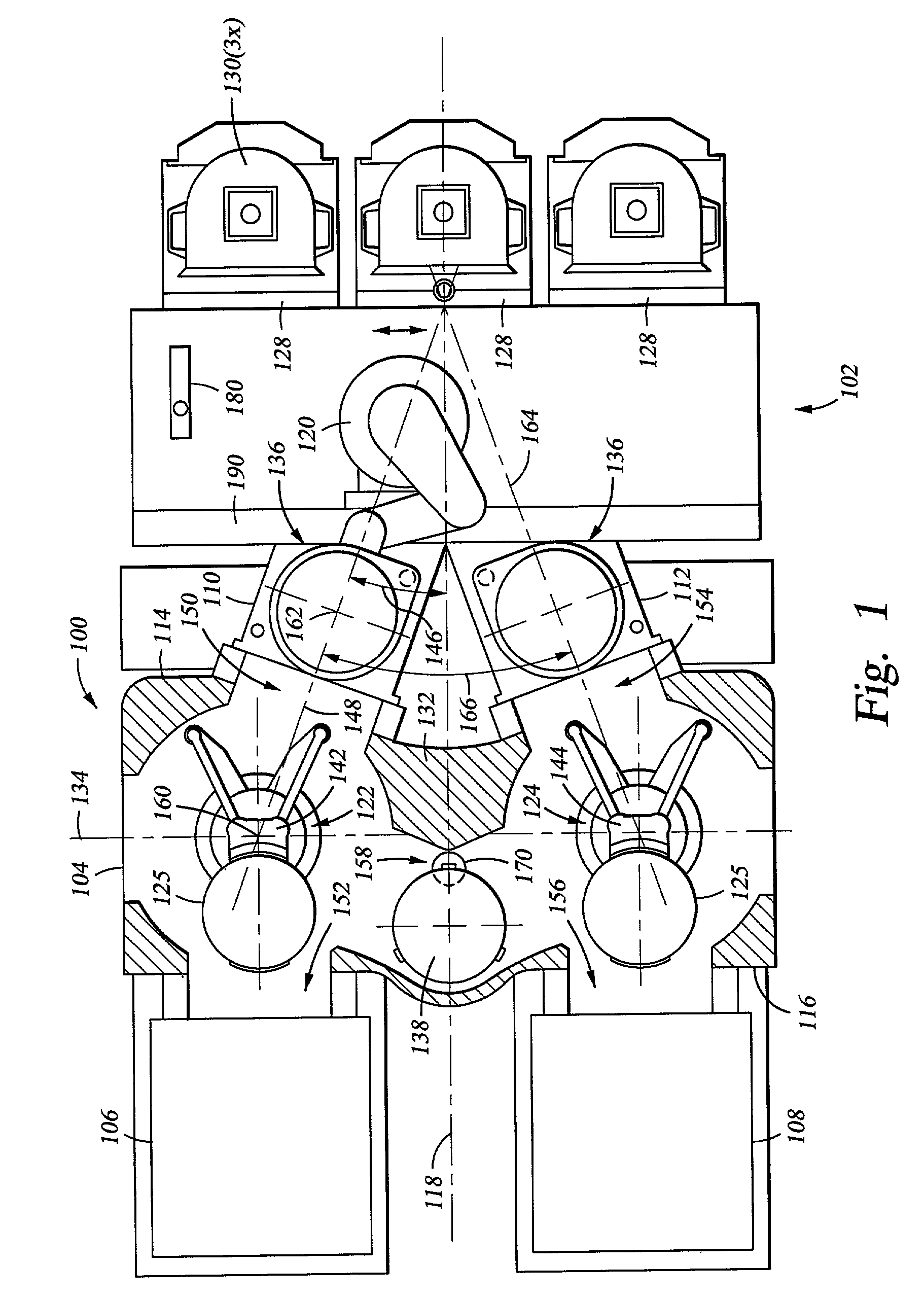
[0022] FIG. 1 depicts one embodiment of a substrate processing system 100 that generally includes a factory interface 102, a first load lock chamber 110, a second load lock chamber 112, a first processing chamber 106, a second processing chamber 108 and a transfer chamber 104. The processing chambers 106, 108 are coupled to the transfer chamber 104. The load lock chambers 110, 112 are coupled between the transfer chamber 104 and the factory interface 102. Substrates 125 are generally transferred from the factory interface 102 through one of the load locks 110, 112 and transfer chamber 104 to one of the processing chambers 106, 108 for processing.

[0023] The factory interface 102 generally includes an interface robot 120, a substrate 180 and a plurality of bays 128 (three are shown). Each bay 128 is adapted to receive a substrate storage cassette 130 that holds a plurality of substrates 125. The factory interface 102 is coupled to the load lock chambers 110, 112 through ports 136 that...


PUM


Abstract

A substrate processing system having a transfer chamber having two processing chambers and two load lock chambers coupled thereto is generally provided. The transfer chamber includes a body having a first transfer area and a second transfer area defined therein on either side of a center axis. A first passage couples one of the load locks with the first transfer area and a second passage couples the other one of the load locks with the second transfer area. The first passage and the second passage form an acute angle about the center axis. A transfer platform is disposed between the first transfer area and the second transfer area. A first transfer robot and a second transfer robot are disposed in the first and second transfer areas, respectively. Each robot is adapted to transfer substrates between the load locks, the transfer platform and a processing chamber.

Description

BACKGROUND OF THE DISCLOSURE[0001] 1. Field of Invention[0002] Embodiments of the invention generally relate to a semiconductor processing system.[0003] 2. Background of Invention[0004] Semiconductor substrate processing is typically performed by subjecting a substrate to a plurality of sequential processes to create devices, conductors and insulators on the substrate. These processes are generally performed in a processing chamber configured to perform a single step of the fabrication process. In order to efficiently complete the entire sequence of processing steps, a number of processing chambers are typically coupled to a central transfer chamber that houses a robot to facilitate transfer of the substrate between the surrounding processing chambers. A semiconductor processing system having this configuration is generally known as a cluster tool, examples of which are the families of PRODUCER.TM., CENTURA.RTM. and ENDURA.RTM. processing systems available from Applied Materials, In...

Claims


Application Information

Patent Timeline
IPC IPC(8): B65G49/07H01L21/00H01L21/677
CPCH01L21/67126H01L21/67184H01L21/67201Y10S414/139H01L21/67745H01L21/67748H01L21/67742
Inventor LEI, LAWRENCE C.KORI, MORIS
Owner APPLIED MATERIALS INC
Why Eureka
Try Eureka