Information recording medium and information recording method
- Summary
- Abstract
- Description
- Claims
- Application Information
AI Technical Summary
Benefits of technology
Problems solved by technology
Method used
Image
Examples
embodiment 1
[0045] [Embodiment 1]
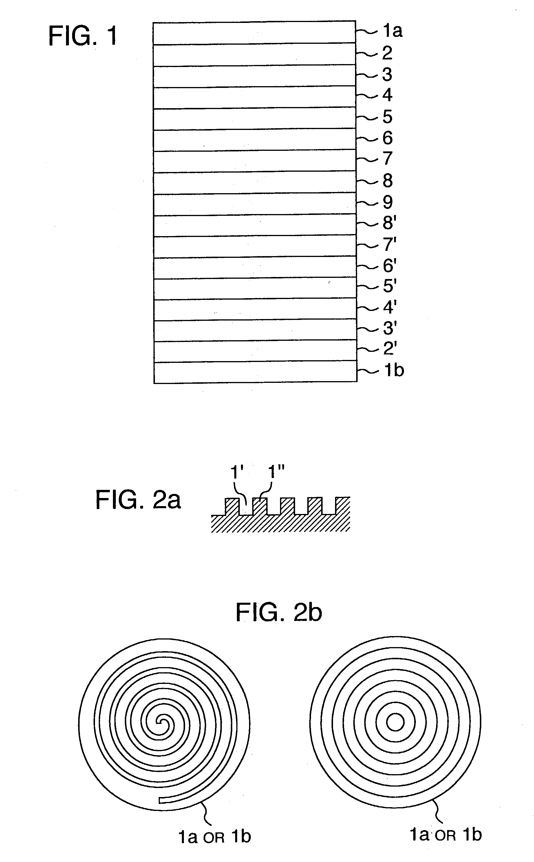
[0046] A substrate 1a formed of transparent material of diameter of 120 mm and thickness of 0.6 mm (for embodiment, polycarbonate resin, glass or the like) with substantially circumferentially extending grooves 1' and lands 1" juxtaposed in the radial direction (that is, concentric or helical) as shown in FIG. 2 was prepared. In one embodiment, the radial distance between the center of the groove 1' and the center of the adjacent land 1' was 0.74 .mu.m. This substrate la was placed in a first sputtering chamber in sputtering equipment having a plurality of sputtering chambers and providing good uniformity and reproducibility of layer thickness. A first overlaid layer 2 of (ZnS).sub.80(SiO.sub.2).sub.-20 (80 and 20 represent mol %) with thickness of 90 nm was formed on the substrate 1a by sputtering in argon gas with a mixture of ZnS and SiO.sub.2 as a target. Then, after this substrate was moved into a second sputtering chamber, a first protective layer 3 of Cr....
embodiment 2
[0055] [Embodiment 2]
[0056] A substrate 1a as in the case of Embodiment 1 was placed in a first sputtering chamber of sputtering equipment having a plurality of sputtering chambers and providing good uniformity and reproducibility of layer thickness. A first overlaid layer 2 of (ZnS).sub.80(Sio.sub.2).sub.-20 (80 and 20 represent mol %) with thickness of 90 nm was formed on the substrate 1a by sputtering in argon gas with a mixture of ZnS and SiO.sub.2 as a target. Then, after this substrate was moved into a second sputtering chamber, a first protective layer 3 of Cr.sub.2O.sub.3 with thickness of 20 nm was deposited by sputtering in argon gas with Cr.sub.2O.sub.3 as a target. Further, after this substrate was moved into a third sputtering chamber, a recording layer 4 was deposited in thickness of 16 nm by sputtering in argon gas with sintered Ag.sub.2.5Ge.sub.20Sb.sub.22.5Te.sub.55 (2.5, 20, 22.5 and 55 represent atomic %) as a target. Then, the substrate was moved into an oxide fo...
embodiment 3
[0063] [Embodiment 3]
[0064] With the same technical limits as Embodiment 1 except that the radial distance between the center of the groove 1' and the center of the neighboring groove was 0.75 .mu.m, the substrate 1a was placed in a first sputtering chamber of sputtering equipment having a plurality of sputtering chambers and providing good uniformity and reproducibility of layer thickness. A first protective layer 2 of (ZnS).sub.80(SiO.sub.2).su-b.20 (80 and 20 represent mol %) with thickness of 90 nm was formed on the substrate 1a by sputtering in argon gas with a mixture of ZnS and SiO.sub.2 as a target. Then, after this substrate was moved into a second sputtering chamber, a recording layer 4 was deposited in thickness of 20 nm by sputtering in argon gas with sintered Ag.sub.4In.sub.7Sb.sub.62Te.s-ub.27 (4, 7, 62 and 27 represent atomic %) as a target. Then, the substrate was moved into an oxide formation chamber and was kept in the environment of oxygen for a certain time perio...
PUM
 Abstract
Description
Claims
Application Information


