Method of spin etching wafers with an alkali solution
- Summary
- Abstract
- Description
- Claims
- Application Information
AI Technical Summary
Problems solved by technology
Method used
Image

Examples
Embodiment Construction
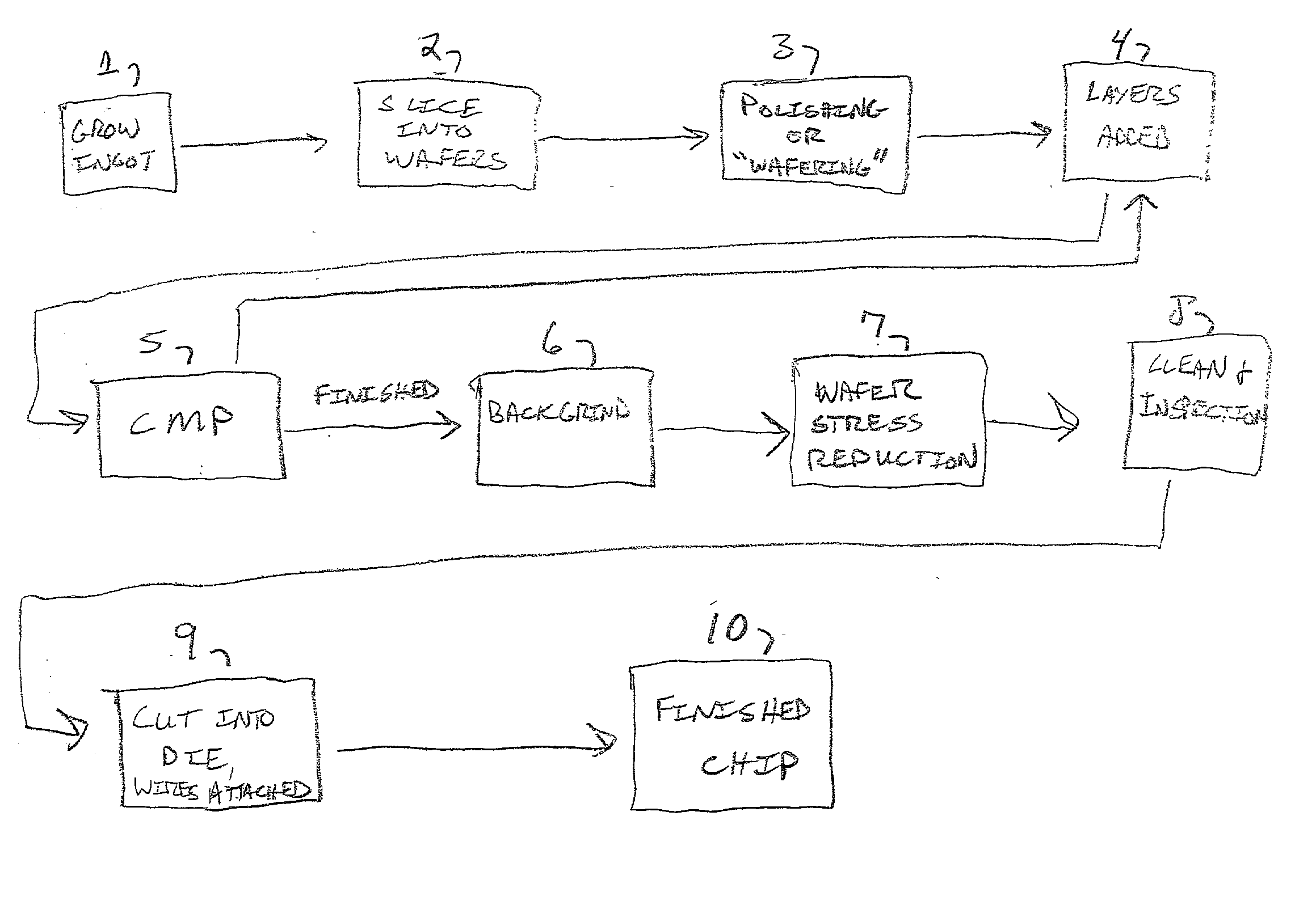
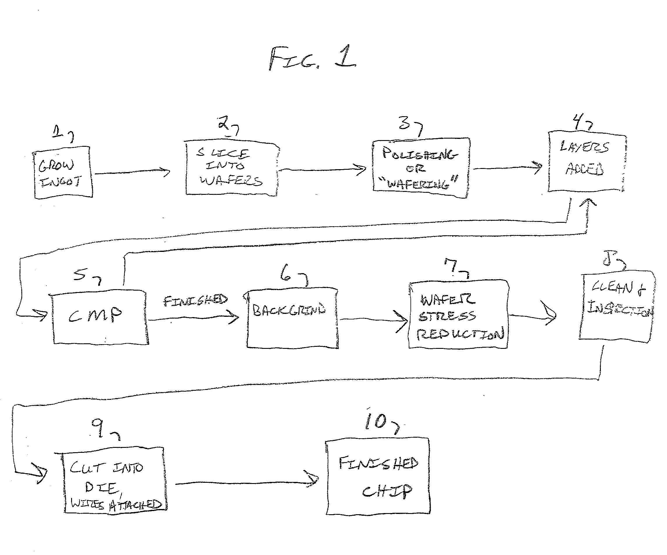
[0015] FIG. 1 is a block diagram of a system for producing integrated chips, including the backgrinding step and the step of spin etching the backside of a wafer with an alkali etch solution. In step 1 silicon is purified and cast into electronic-grade ingots. The ingots are then converted into high purity, single crystal silicon by growing a crystal silicon structure. In step 2 the ingot is sliced into wafers using a diamond saw, with each wafer being approximately {fraction (1 / 40)} thick. In step 3 each wafer is polished, lapped smooth, damage decorated with acid to reveal hidden defects, and may be ground either over the wafer surface or at its edges. After the polishing processing, also known as wafering, is complete the new prime wafer is ready to have integrated circuits built upon it. In steps 4 and 5, integrated circuits are built onto the front side of the wafer. In step 4 at least one layer of material is deposited onto the silicon wafer substrate. Then, in step 5, a CMP p...
PUM
 Abstract
Description
Claims
Application Information
 - R&D Engineer
- R&D Manager
- IP Professional
- Industry Leading Data Capabilities
- Powerful AI technology
- Patent DNA Extraction
Browse by: Latest US Patents, China's latest patents, Technical Efficacy Thesaurus, Application Domain, Technology Topic.
© 2024 PatSnap. All rights reserved.Legal|Privacy policy|Modern Slavery Act Transparency Statement|Sitemap