Phosphor thin film, preparation method, and EL panel

a technology of phosphor and thin film, applied in the field of phosphor thin film, preparation method, and el panel, can solve the problems of unsuitable color display, green and blue suffer from emission luminance, emission efficiency and color purity, and color el panel has not reached the commercial stag

Inactive Publication Date: 2003-08-07
IFIRE IP CORP
View PDF29 Cites 15 Cited by
  • Summary
  • Abstract
  • Description
  • Claims
  • Application Information

AI Technical Summary

Problems solved by technology

Thin-film EL displays using sulfide phosphor thin films are fully reliable and resistant to environment, but at present regarded unsuitable as color displays because EL phosphors required to emit light in the primary colors of red, green and blue have poor characteristics.
These phosphor thin films capable of emitting light in the primaries of red, green and blue suffer from problems of emission luminance, emission efficiency and color purity.
Thus color EL panels have not reached the commercial stage.
These thiogallate base phosphors are satisfactory in color purity, but suffer from difficulty to form a thin film of uniform composition because of the multi-component composition.
It is believed that thin films of quality are not obtainable because of poor crystallinity resulting from inconvenient composition control, formation of defects resulting from sulfur removal, and admittance of impurities; and these factors lead to a failure to increase the luminance.
This gives rise to several problems.
The substrate material is limited because the substrate must be noticeably heat resistant; diffusion of elements occurs from the substrate or adjacent layer (insulating layer or the like) to the phosphor thin film; interlaminar flatness is compromised; interlaminar separation occurs during high-temperature annealing; pixels are destroyed by surface diffusion during high-temperature annealing; and a thermal guard must be provided on the annealing apparatus for high-temperature annealing, which adds to the expense.
This means that in a full color panel requiring three colors RGB to be disposed within it, the conditions under which the respective phosphor thin films are formed for providing the desired emission characteristics differ among them, rendering panel manufacture difficult.
However, this EL...

Method used


Image

  • Phosphor thin film, preparation method, and EL panel
  • Phosphor thin film, preparation method, and EL panel
  • Phosphor thin film, preparation method, and EL panel

Examples


example 1

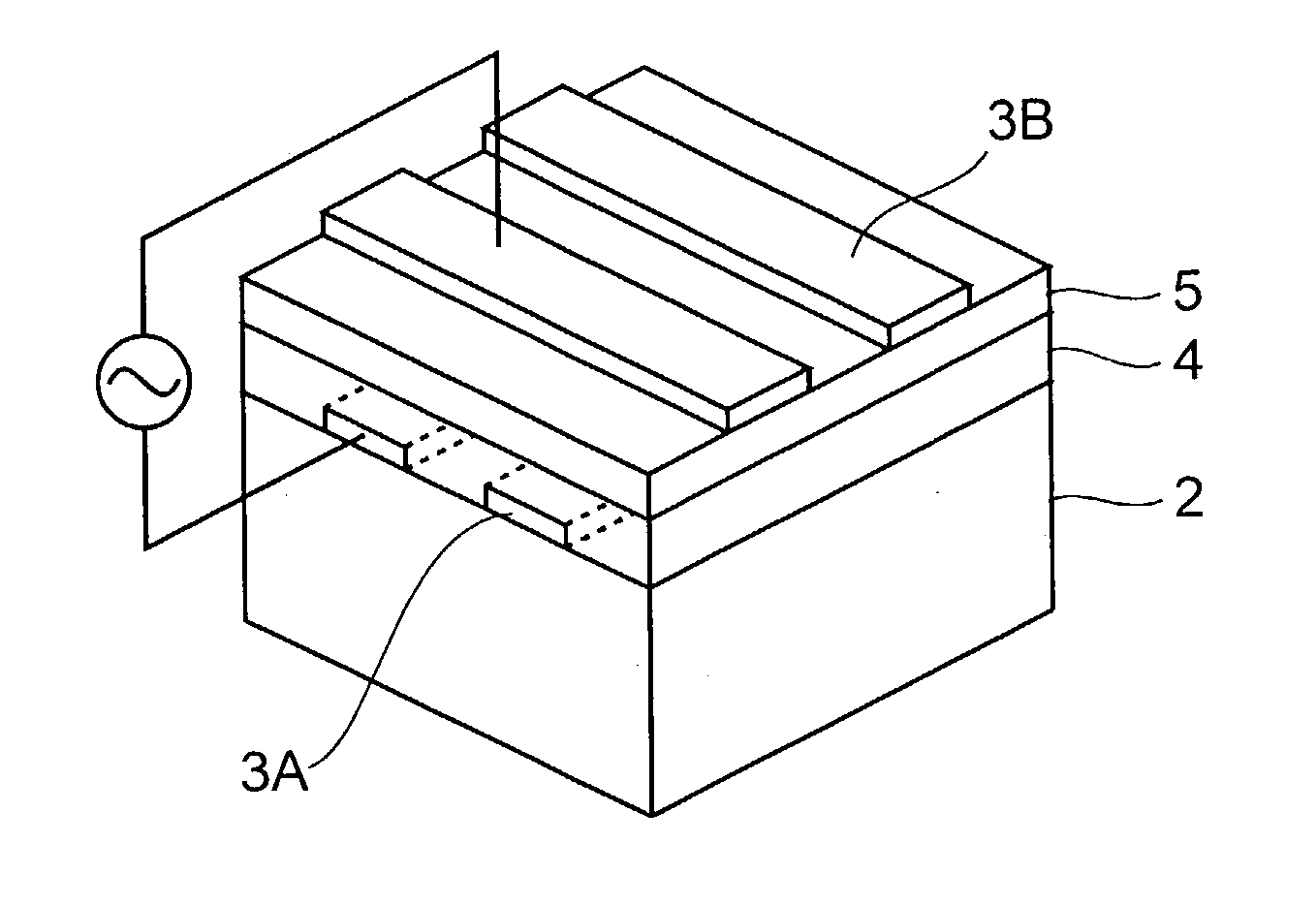
[0102] An EL device (or panel) was fabricated using a phosphor thin film according to the invention. The EL device basically has the structure shown in FIG. 4.

[0103] For the substrate 2 and insulating layer 4, BaTiO.sub.3--PbTiO.sub.-3 base dielectric material having a permittivity of 5,000 was commonly used. For the lower electrode 3A, Pd was used. On fabrication, a sheet of the substrate 2 was formed, and pastes for the lower electrode 3A and insulating layer 4 were screen printed thereon to form green sheets, which were co-fired. The surface of the insulating layer 4 was polished to a thickness of 30 .mu.m. On the insulating layer 4, a BaTiO.sub.3 coating was formed by sputtering as a barrier layer to a thickness of 400 nm. This was annealed in air at 700.degree. C.

[0104] On the barrier layer, a thin film laminate having the structure of Al.sub.2O.sub.3 film (50 nm) / ZnS thin film (200 nm) / phosphor thin film (200 nm) / ZnS thin film (200 nm) / Al.sub.2O.sub.3 film (50 nm) was formed a...

example 2

[0124] An EL device was fabricated as in Example 1 except that a BaS pellet was used instead of the SrS pellet, a Al.sub.2S.sub.3 pellet was used instead of the Ga.sub.2S.sub.3 pellet, and a phosphor thin film of Zn.sub.vBa.sub.xAl.sub.yO.sub.zS.sub.w:Eu having a thickness of 300 nm was formed. The phosphor thin film was analyzed for composition by fluorescent x-ray analysis, finding an atomic ratio (arbitrary unit) as shown below.

1 Zn: 1.40 Ba: 8.86 Al: 16.45 O: 6.88 S: 26.50 Eu: 0.44

[0125] This indicates that the atomic ratios in Zn.sub.vBa.sub.xAl.sub.yO.-sub.zS.sub.w:Eu are:

[0126] v / x=0.16,

[0127] y / x=1.86,

[0128] z / (z+w)=0.21, and

[0129] (v+x+3y / 2) / (z+w)=1.05.

[0130] The Eu content is 5 at % based on Ba.

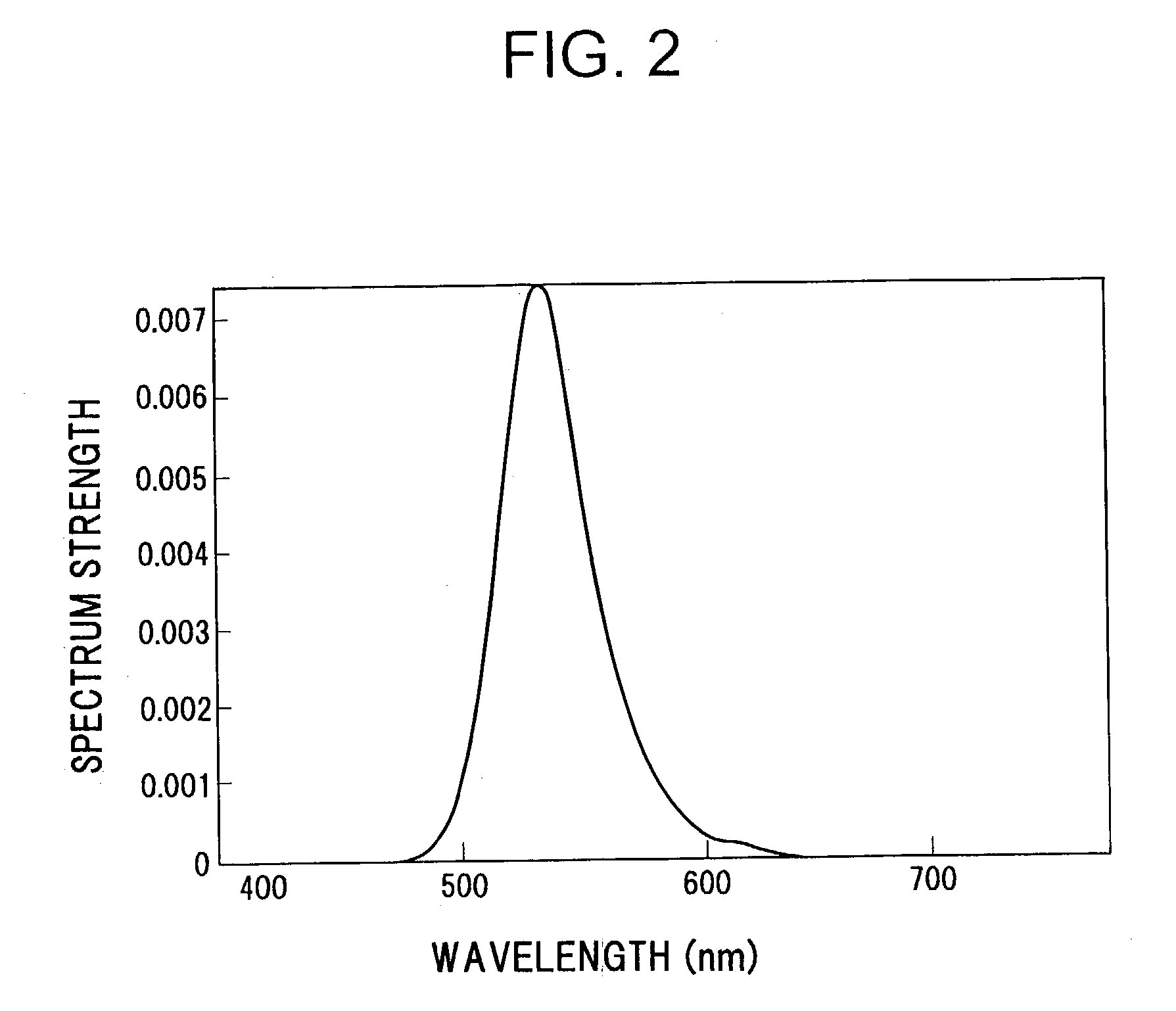
[0131] The emission performance of the EL device was examined as in Example 1. Blue light emission having a luminance of 700 cd / m.sup.2 was produced in a reproducible manner. For comparison purposes, an EL device was similarly fabricated except that a phosphor thin film of Zn-free B...

example 3

[0133] EL devices were fabricated as in Example 1 except that the values of v / x and y / x in the phosphor thin film of Zn.sub.vSr.sub.xGa.sub.yO.sub-.zS.sub.w:Eu were changed as shown in Table 1. The luminance of these EL devices was measured as in Example 1, with the results shown in Table 1.

2 TABLE 1 Device Luminance No. v / x y / x (cd / m.sup.2) 1 1.27 2.52 631 2 0.05 1.78 1742 3 0.35 2.48 655 4 0.27 1.73 1711 5 0.15 1.86 2170

[0134] The advantages of the invention are evident from Table 1. The luminance of the phosphor thin film is improved by introducing Zn therein. A very high luminance is achieved when v / x is from 0.001 to 1 and y / x is from 1.6 to 1.99.

[0135] In an additional run, phosphor thin films were formed using Ba as element A, In as element B and Eu as the luminescent center, and annealed at a relatively low temperature of 700.degree. C. It was confirmed that the addition of Zn to the phosphor thin film achieved an improvement in the luminance of red light emission.

Benefits o...


PUM

PropertyMeasurementUnit
Angleaaaaaaaaaa
Angleaaaaaaaaaa
Angleaaaaaaaaaa

Abstract

In a phosphor thin film comprising a matrix material and a luminescence center, the matrix material has the compositional formula: MIIvAxByOzSw wherein MII is Zn, Cd or Hg, A is Mg, Ca, Sr, Ba or rare earth element, B is Al, Ga or In, and atomic ratios v, x, y, z and w are 0.005<=v<=5, 1<=x<=5, 1<=y<=15, 0<z<=30, and 0<w<=30. The phosphor thin film of quality is formed at low cost by a low-temperature process, enabling manufacture of full-color EL panels.

Description

[0001] 1. Technical Field[0002] This invention relates to a phosphor thin film for use in electroluminescent (EL) devices, a method of preparing the same and an EL panel using the same.[0003] 2. Background Art[0004] In the recent years, active research works have been made on thin-film EL devices as small-size or large-size, lightweight flat display panels. A monochromatic thin-film EL display using a phosphor thin film of manganese-doped zinc sulfide capable of emitting yellowish orange light has already become commercially practical as a double insulation structure using thin-film insulating layers 4A and 4B as shown in FIG. 5. In FIG. 5, a predetermined pattern of lower electrodes 3A is formed on a glass substrate 2, and a dielectric thin film is formed as a lower insulating layer 4A on the lower electrode-bearing substrate 2. On the lower insulating layer 4A, a light-emitting layer 5 in the form of a phosphor thin film and an upper insulating layer 4B are successively formed. On...

Claims


Application Information

Patent Timeline
IPC IPC(8): H05B33/10C09K11/00C09K11/08C09K11/62C09K11/64C09K11/77C09K11/84C09K11/86H05B33/14
CPCC09K11/7729C09K11/773C09K11/7731Y10S428/917C09K11/7789H05B33/14C09K11/7734C09K11/62
Inventor YANO, YOSHIHIKOOIKE, TOMOYUKITAKAHASHI, MASAKINAGANO, KATSUTO
Owner IFIRE IP CORP
Why Eureka
Try Eureka