Low-power, low-noise CMOS amplifier
- Summary
- Abstract
- Description
- Claims
- Application Information
AI Technical Summary
Benefits of technology
Problems solved by technology
Method used
Image

Examples
Embodiment Construction
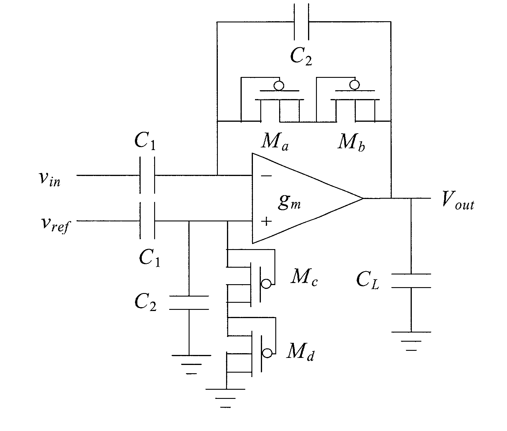
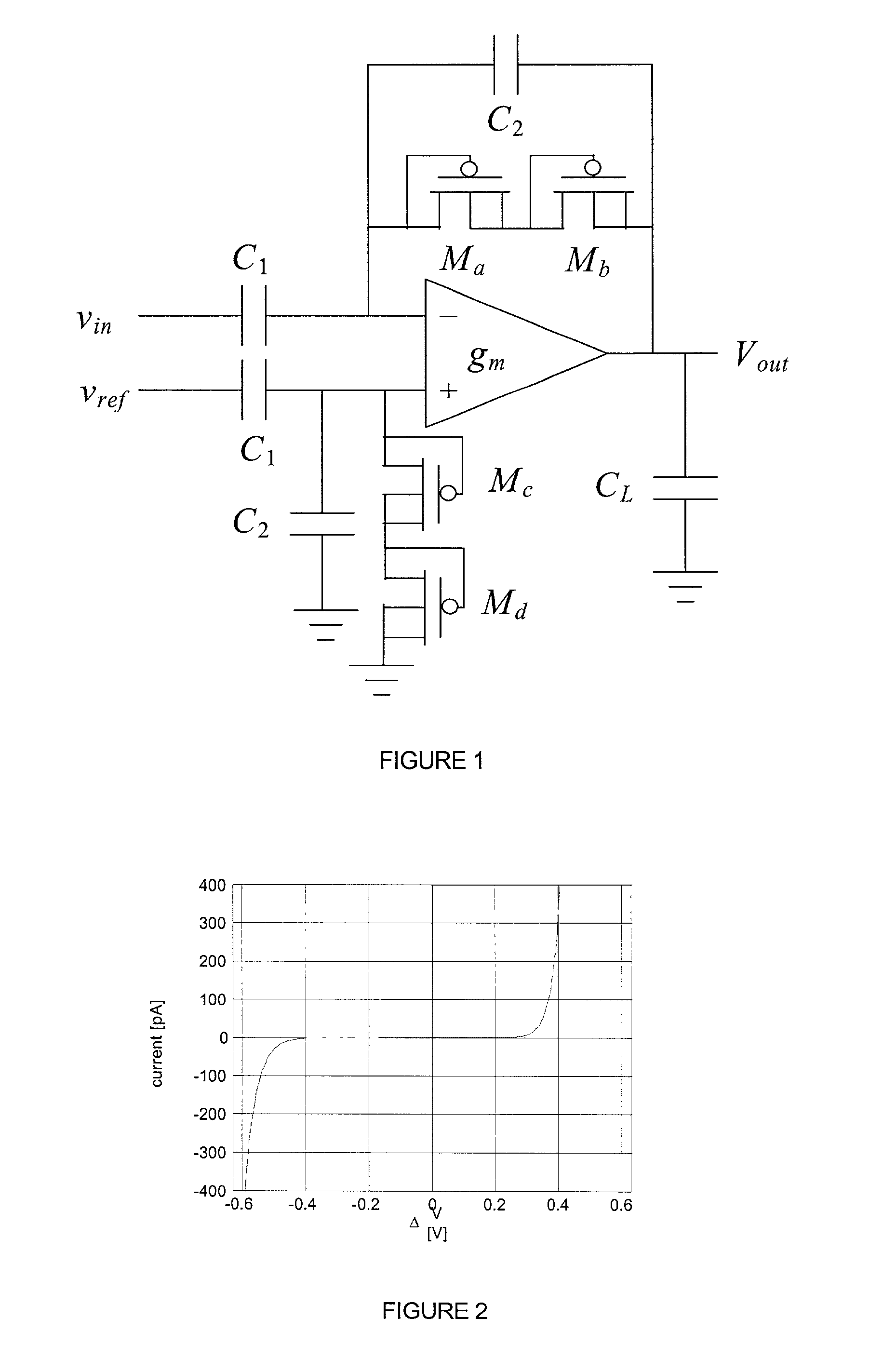
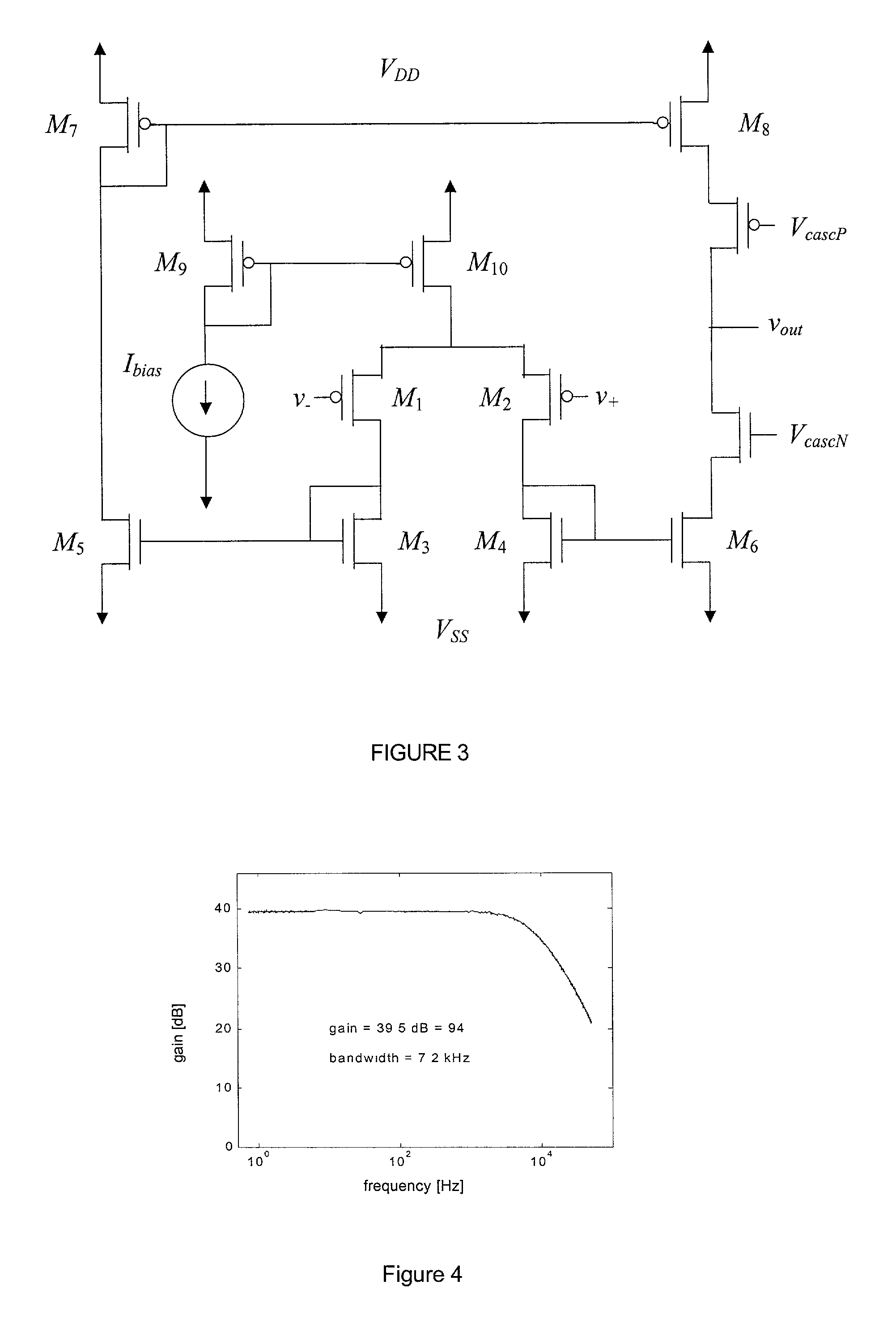
[0043] An amplifier in a 1.5 .mu.m 2-poly commercially-available CMOS process was fabricated to be a fully-integrated circuit of dimensions 250 .mu.m by 700 .mu.m on a chip with dimensions of 2.2 mm by 2.2 mm. No external components such as capacitors or resistors are necessary for the circuit operation; all necessary circuit components are contained on the chip as an integrated circuit having dimensions of less than 1 mm by 1 mm. The amplifier was designed for a gain of 100, setting C.sub.1 to 20 pF and C.sub.2 to 200 fF. FIG. 4 shows the measured amplifier transfer function from 0.7 Hz to 50 kHz. The midband gain was measured to be 39.5 dB, slightly lower than the designed specification of 40 dB. This discrepancy is likely caused by fringing fields on the small C.sub.2 capacitors, yielding a larger capacitance than designed. FIG. 5 shows the output of the amplifier in response to a 0.006 Hz square wave. Based on the slow adaptation of the output, the low-frequency cutoff f.sub.L w...
PUM
 Abstract
Description
Claims
Application Information
 - R&D Engineer
- R&D Manager
- IP Professional
- Industry Leading Data Capabilities
- Powerful AI technology
- Patent DNA Extraction
Browse by: Latest US Patents, China's latest patents, Technical Efficacy Thesaurus, Application Domain, Technology Topic.
© 2024 PatSnap. All rights reserved.Legal|Privacy policy|Modern Slavery Act Transparency Statement|Sitemap