Driving method for electro-optical device, driving circuit therefor, electro-optical device, and electronic apparatus

a driving circuit and electrooptical technology, applied in the direction of electric digital data processing, instruments, computing, etc., can solve the problems of increased power consumption, increased overall device cost, and difficulty in high-quality display, so as to suppress display non-uniformity, reduce data transfer rate, and suppress display non-uniformity

Inactive Publication Date: 2003-08-21
SEIKO EPSON CORP
View PDF6 Cites 23 Cited by
  • Summary
  • Abstract
  • Description
  • Claims
  • Application Information

AI Technical Summary

Benefits of technology

[0178] As described above, according to the present invention, display nonuniformity resulting from unevenness in circuit characteristic, various wiring resistances, etc., can be reduced, and it is not necessary to sequentially select all scanning lines in each subfield, but is sufficient to select only the scanning line in which the reference time of weighting has arrived, thereby reducing the data transfer rate in one subfield. This also makes it possible to reduce the power consumption.

Problems solved by technology

This requires a D / A converting circuit, an op amp, etc., as peripheral circuits of the electro-optical device, leading to increased cost of the overall device.
In addition, display nonuniformity is caused by unevenness in characteristics of the D / A converting circuit, the op amp, etc., in various wiring resistances, etc., leading to a problem in that it is extremely difficult to perform high-quality display.
There are also problems of increased power consumption resulting from the D / A converting circuit, op amp, etc.

Method used


Image

  • Driving method for electro-optical device, driving circuit therefor, electro-optical device, and electronic apparatus
  • Driving method for electro-optical device, driving circuit therefor, electro-optical device, and electronic apparatus
  • Driving method for electro-optical device, driving circuit therefor, electro-optical device, and electronic apparatus

Examples


Embodiment Construction

[0056]

[0057] Before an electro-optical device according to an embodiment of the present invention is described, first, the theoretical assumptions of gray scale display according to the present invention is briefly described. In general, in a liquid crystal device using liquid crystal as an electro-optical material, the relationship between an effective voltage value applied to the liquid crystal layer forming a pixel (when the applied on voltage is constant and the pulse width of the on voltage is changed) and the relative transmittance (or reflectance) is as shown in FIG. 5, if a normally black mode is taken as an example where black display is performed while no voltage is applied. Specifically, the relationship is that the transmittance (or reflectance) varies as the effective voltage value applied to the liquid crystal layer ranges from A (V) to B (V). The relative transmittance, as used herein, is determined by normalizing the minimum and maximum values of the amount of trans...


PUM


Abstract

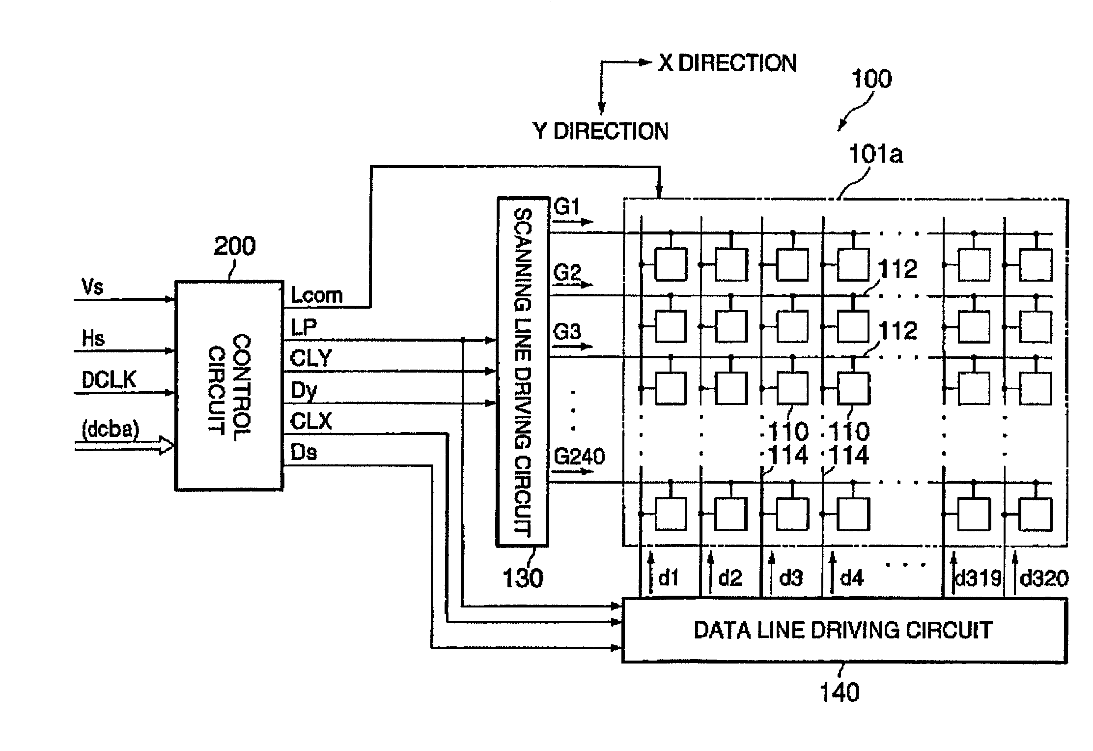
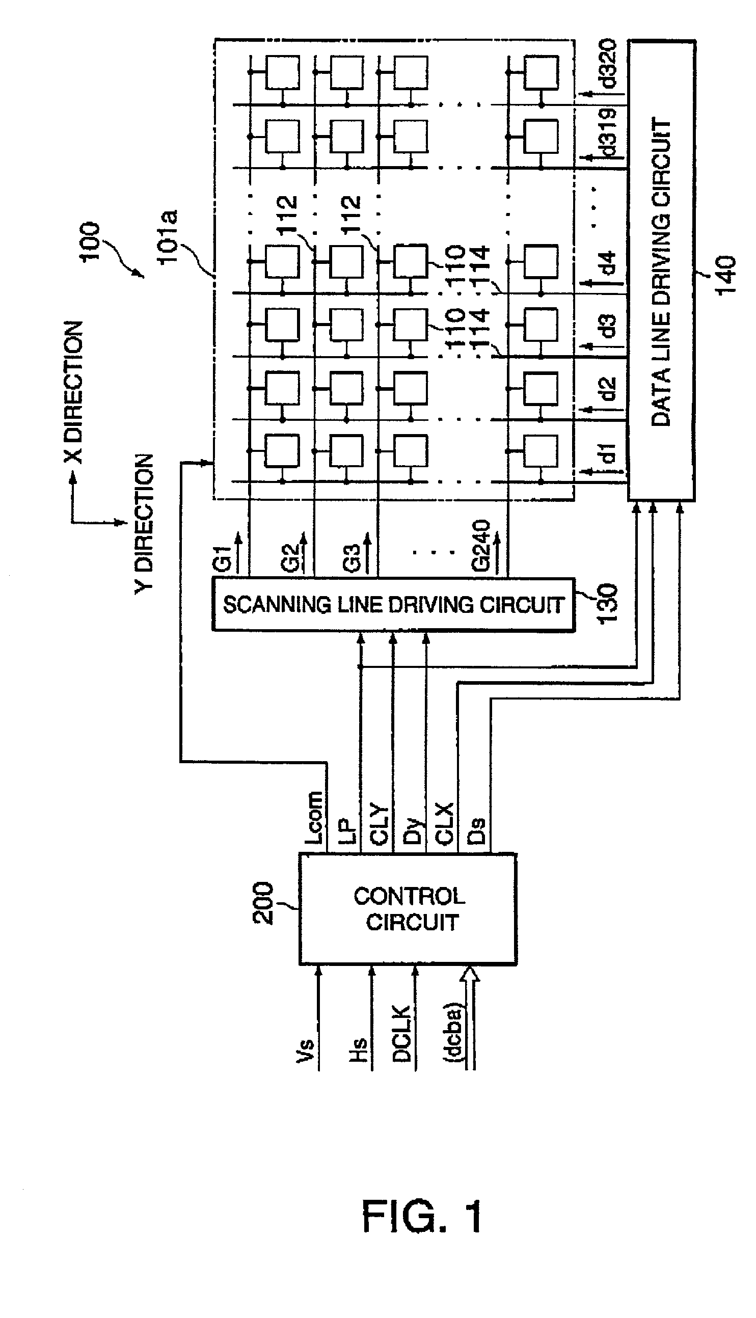
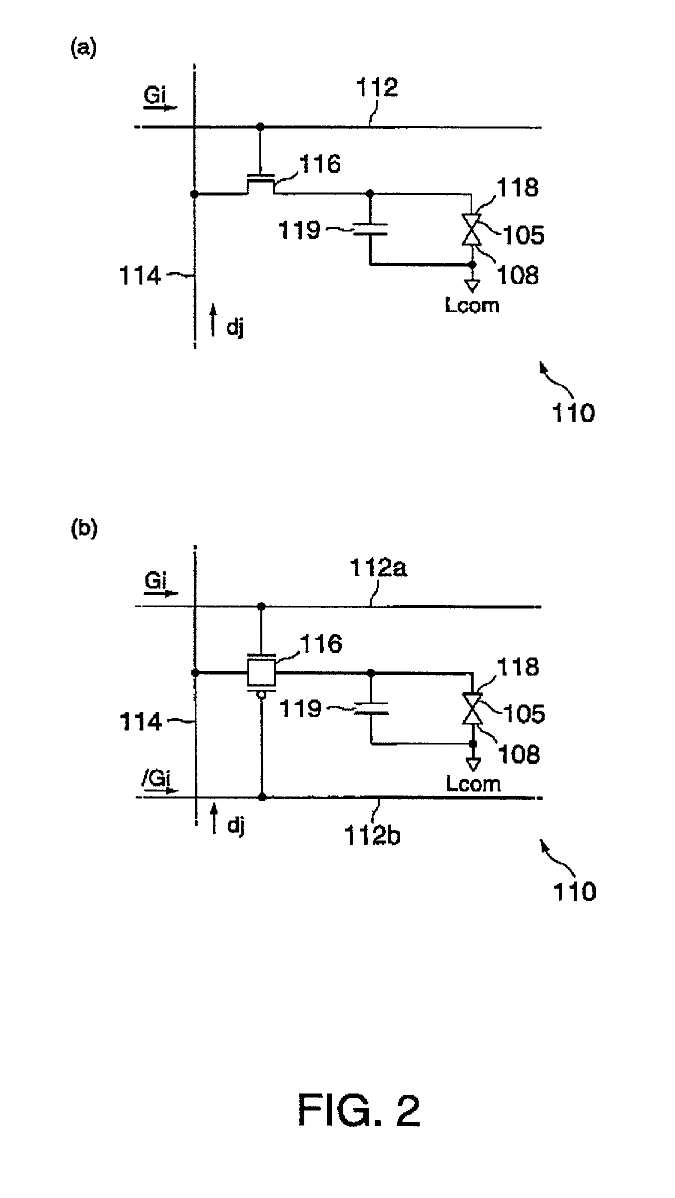
To reduce the data transfer rate in one subfield while suppressing display nonuniformity, a pixel positioned corresponding to each intersection between a plurality of scanning lines and a plurality of data lines is turned on or off in subfields sf1 to sf17, into which one field (1f) is divided, according to weighting of gray scale data (dcba) indicating the gray scale level of that pixel, and the reference time of weighting for the gray scale data is shifted every scanning line and every subfield.

Description

[0001] The present invention relates to a driving method for an electro-optical device, in which gray scale display is performed by temporal modulation, a driving circuit therefor, an electro-optical device, and electronic apparatus.[0002] Electro-optical devices, such as liquid crystal display devices using liquid crystal as an electro-optical material, have been widely used, as alternative display devices to cathode-ray tubes (CRTs), for display units of various kinds of information processing apparatuses, liquid crystal television sets, etc. Here, a conventional electro-optical device is formed of, for example, an element substrate incorporating pixel electrodes which are arranged into a matrix, switching elements coupled with the pixel electrodes, etc., an opposing substrate having counter electrodes formed thereon which face the pixel electrodes, and liquid crystal as an electro-optical material which is filled between the two substrates. In such a structure, when a single scan...

Claims


Application Information

Patent Timeline
Patent Type & Authority Applications(United States)
IPC IPC(8): G09G3/20G09G3/36
CPCG09G3/20G09G3/2022G09G2310/02G09G3/3659G09G2300/0857G09G3/3648
Inventor ITO, AKIHIKO
Owner SEIKO EPSON CORP
Why Eureka
Try Eureka