
Method for producing a superconducting circuit

a superconducting circuit and superconducting technology, applied in the direction of conductive materials, conductors, electrical equipment, etc., can solve the problems of large cooling apparatus, unfavorable chemical reactions, and the need to cool the device to very low temperatures during operation, so as to reduce the electrical conductivity, reduce the spatial and crystallographic structure of the film, and reduce the effect of heat dissipation

Inactive Publication Date: 2003-12-25
IMS NANOFABTION
View PDF8 Cites 3 Cited by
  • Summary
  • Abstract
  • Description
  • Claims
  • Application Information

AI Technical Summary

Benefits of technology

The present invention offers advantages compared to previous methods for creating patterns in HTS films. Instead of using a photosensitive resin called photoresist, which requires curbing the film in physical contact with etchants and results in damage to the surface, the invention uses a contactless method based on the principle of weak coupling between superconducting and non-Superconducting Phases (NSPs). Ions, particularly light ones, are used to inhibit superconductivity without affecting the crystallographic structure of the film. The resulting nanostructure prevents unwanted interactions with adjacent layers during operation and enables precise control of interfaces between NSPs. Additionally, the invention preserves the ability to grow additional layers on the same substrate. These technical advancements make the invention ideal for creating stable and reliable electronic devices.

Problems solved by technology

The technical problem addressed in this patent is how to create precise patterns of superconducting circuits inHTS films without compromising the crystal structure and causing mechanical stress at interfaces. Prior methods involved heavy ion irradiation and were restricted to relatively narrowly focused laser lines. However, this new approach uses light ions and takes advantage of the fact that they induce less damage to the host material compared to heavier ions. By controlling the amount of light ions and the duration of the experiment, researchers discovered that there is a critical density threshold for achieving complete inhibition of superconductivity. Using these thresholds, the method can leave the crystal structure largely unaffected and allow for the growth of multiple layers of HTS or other materials on the surface of the film.

Method used


Image

  • Method for producing a superconducting circuit
  • Method for producing a superconducting circuit
  • Method for producing a superconducting circuit

Examples


Embodiment Construction

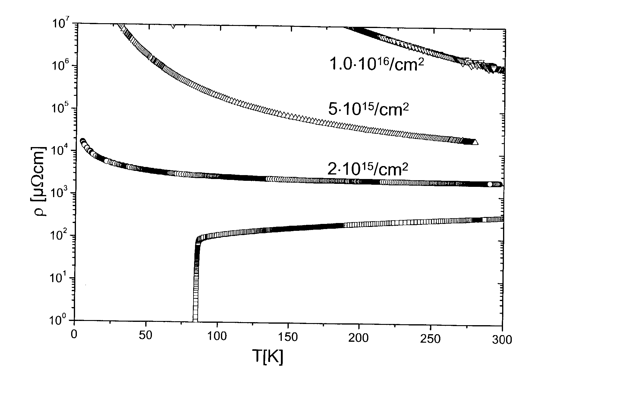
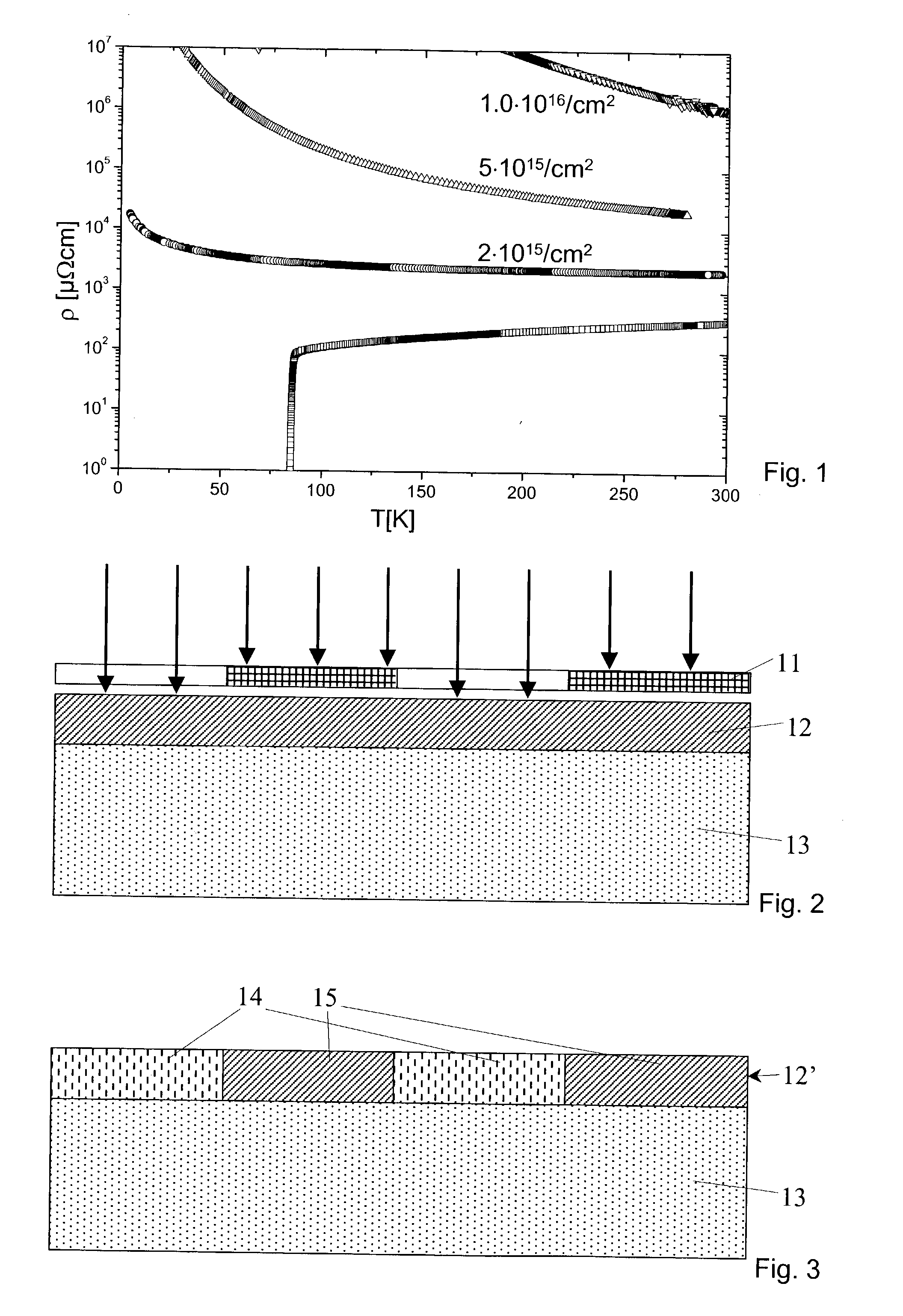
[0034] FIG. 1 shows the change of the resistivity, in .mu..OMEGA.cm, of a representative HTS, namely YBCO, as a function of the temperature at different irradiation doses, namely the initial resistivity function after preparation (square symbols) and after subsequent, cumulative irradiation with 75 keV He.sup.+ ions with total dose 2.multidot.10.sup.15, 5.multidot.10.sup.15, and 1.0.multidot.10.sup.16 ions / cm.sup.2, respectively. The YBCO film was generated on a MgO substrate by pulsed laser deposition and had a thickness of 100 nm; after deposition, the film was covered with a silicon oxide protective layer of a thickness of about 175 nm by means of electron-beam evaporation of SiO.sub.2 granulate. The graph demonstrates the inhibition of superconductivity and the increase of the resistivity after ion irradiation, and that already with a low ion dose--in this example with about 2.multidot.10.sup.15 ions / cm.sup.2 (circle symbols)--it is possible to suppress superconducting behavior ...


PUM


Abstract

For producing a superconducting circuit, a film (12) consisting of a cuprate superconductor material is generated on a substrate (13), wherein the superconductor material is in the superconducting state at an operating temperature of the superconducting circuit to be produced, and then the film is irradiated by projecting an energetic ion radiation onto the film through a mask (11) positioned at a distance from the film and protecting selected areas of the film from being irradiated, the mask comprising a structure pattern transparent to the ion radiation but otherwise opaque to the ion radiation. Areas (14) not protected by the mask are irradiated with an ion dose being sufficiently low to avoid degradation of the crystal structure of the first film but being sufficient to inhibit superconductivity of the film with respect to the operating temperature; ion doses are preferably in the range of 0.8.10<15 >and 2.10<15 >ions/cm<2 >or below. The areas (15) of the film thus protected from irradiation form film portions which, at least at the operating temperature, act as a superconducting circuit.

Description


Claims


Application Information

Patent Timeline
Owner IMS NANOFABTION
Learn More