Semiconductor integrated circuit with a test circuit

a technology of integrated circuit and test circuit, which is applied in the direction of semiconductor devices, solid-state devices, instruments, etc., can solve the problems of long time expended in inputting and outputting test data, enlarge the number of scan registers to constitute the scan chain, and increase the number of scan registers

Inactive Publication Date: 2004-03-11
LAPIS SEMICON CO LTD
View PDF10 Cites 76 Cited by
  • Summary
  • Abstract
  • Description
  • Claims
  • Application Information

AI Technical Summary

Problems solved by technology

The test circuit of such a shift scan system, however, has had the problem that, as the number of the logic circuit blocks becomes larger, the number of the scan registers to constitute the scan chain enlarges more, so a long time is expended in inputting and outputting the test data.
As stated before, the semiconduct

Method used


Image

  • Semiconductor integrated circuit with a test circuit
  • Semiconductor integrated circuit with a test circuit
  • Semiconductor integrated circuit with a test circuit

Examples


first embodiment

[0016] (First Embodiment)

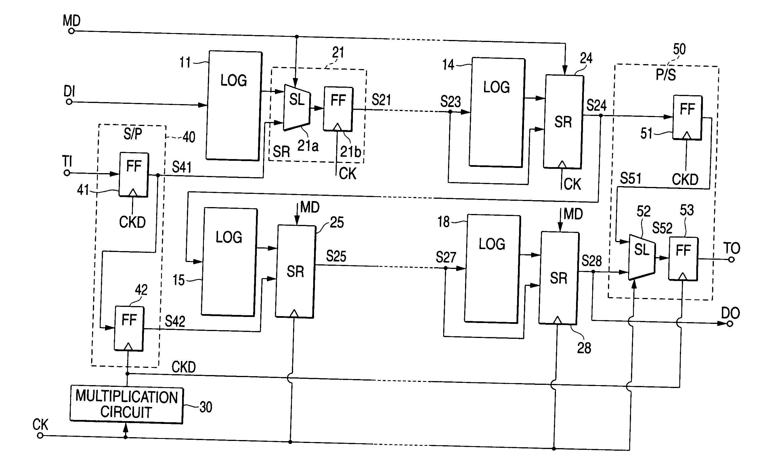
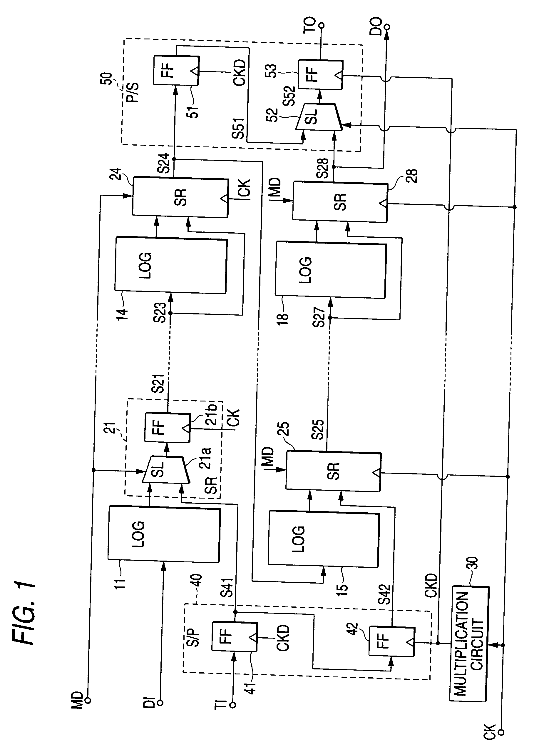
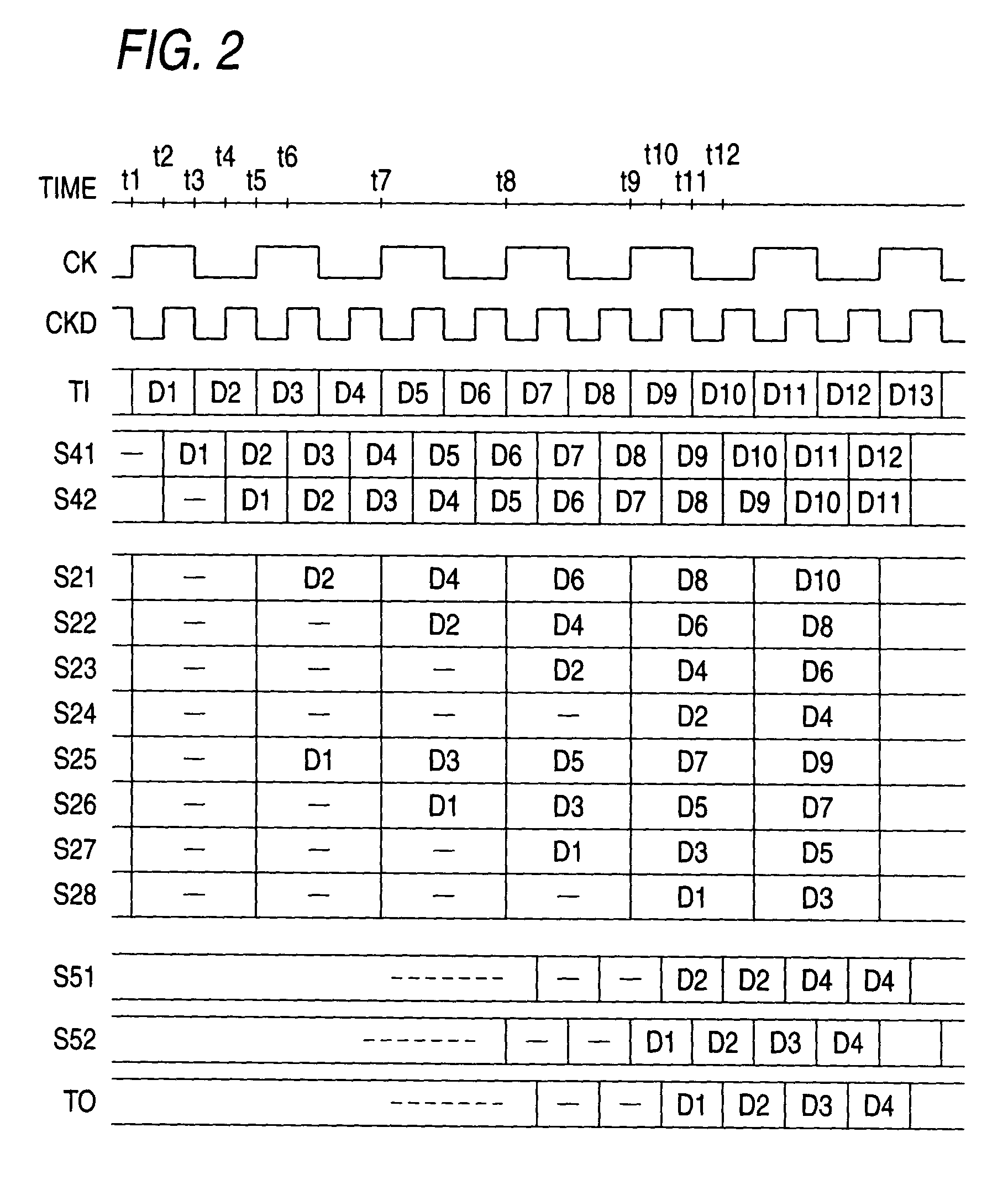
[0017] FIG. 1 is a block diagram of a semiconductor integrated circuit showing the first embodiment of the present invention.

[0018] The semiconductor integrated circuit has a test circuit of shift scan system, and it includes (for example, eight) logic circuit blocks 11-18 which perform the functional operations of the integrated circuit, scan registers 21-28 which are respectively connected to the output nodes of the logic circuit blocks 11-18, a multiplication circuit 30 which generates from a clock signal CK a multiplied clock signal CKD at a frequency being double higher than that of the clock signal CK, a serial / parallel conversion circuit (S / P) 40, and a parallel / serial conversion circuit (P / S) 50.

[0019] All the scan registers 21-28 are similarly constructed. As shown in the scan register 21 by way of example, each scan register is configured of a selector (SL) 21a which changes over input signals in accordance with a mode signal MD, and a flip-flop (F...

second embodiment

[0043] (Second Embodiment)

[0044] FIG. 3 is a block diagram of a semiconductor integrated circuit showing the second embodiment of the present invention.

[0045] The semiconductor integrated circuit includes m.times.n logic circuit blocks 10.sub.i, j (where i=1-m and j=1-n hold) which perform the functional operations of the integrated circuit, scan registers 20.sub.i, j which are connected among the logic circuit blocks 10.sub.i, j, a multiplication circuit 35 which generates from a clock signal CK a multiplied clock signal CKD at a frequency being m times higher than that of the clock signal CK, a serial / parallel conversion circuit 45, and a parallel / serial conversion circuit 55.

[0046] The m.times.n logic circuit blocks 10.sub.i, j as well as the scan registers 20.sub.i, j are divided every n constituents, whereby m sets of divisional chain circuits are constructed.

[0047] The divisional chain circuit of the first set is so constructed that the logic circuit blocks 10.sub.1, 1-10.sub....


PUM


Abstract

A shift scan chain includes logic circuit blocks 11-18 and scan registers 21-28 connected at stages succeeding them. The shift chain is divided into divisional chains including the scan registers 21-24 and the scan registers 25-28. In the test operation mode of a semiconductor integrated circuit, test input data TI are supplied in synchronism with a multiplied clock signal CKD at a frequency twice of that of a clock signal CK. The test input data TI are converted by a serial/parallel conversion circuit 40 into parallel data S41 and S42, which are respectively supplied to the head scan registers 21 and 25 of the corresponding divisional chains. The length of each divisional chains becomes ½, and a test time period can be shortened.

Description

[0001] 1. Field of the Invention[0002] The present invention relates to a semiconductor integrated circuit having a test circuit based on scan registers, and a method of testing the semiconductor integrated circuit.[0003] 2. Description of the Related Art[0004] As a technique for testing a semiconductor integrated circuit, there has been one called "shift scan system" wherein scan registers are inserted among logic circuit blocks which perform the functional operations of the integrated circuit, and in the test mode of the integrated circuit, the scan registers are connected in the shape of a chain so as to supply testing data to the respective logic circuit blocks and to derive output data from them.[0005] The test circuit of such a shift scan system, however, has had the problem that, as the number of the logic circuit blocks becomes larger, the number of the scan registers to constitute the scan chain enlarges more, so a long time is expended in inputting and outputting the test ...

Claims


Application Information

Patent Timeline
IPC IPC(8): G01R31/3185G01R31/28H01L21/822H01L27/04
CPCG01R31/318572G01R31/318552
Inventor OBARA, TERUHISA
Owner LAPIS SEMICON CO LTD
Why Eureka
Try Eureka