High frequency circuit element and high frequency circuit module

Inactive Publication Date: 2004-03-25
PANASONIC CORP
View PDF6 Cites 26 Cited by
  • Summary
  • Abstract
  • Description
  • Claims
  • Application Information

AI Technical Summary

Benefits of technology

0077] Note that as shown in FIG. 2(b), the pair of transmission lines 4 does not have to be inserted separately to the longer side walls of the shielding conducto

Problems solved by technology

First, since the dielectric member is used without being shielded, high-frequency signals (electromagnetic waves) from the dielectric member are emitted. The signal emission may cause an increase in the loss of a resonator, i.e., a reduction in the Q value of the resonator. Moreover, by the emitted electromagnetic waves, the dielectric member may be coupled with other circuits disposed on a substrate to make circuit operation unstable. Furthermore, in order to suppress the coupling between the dielectric member and other circuits by the emitted electromagne

Method used


Image

  • High frequency circuit element and high frequency circuit module
  • High frequency circuit element and high frequency circuit module
  • High frequency circuit element and high frequency circuit module

Examples


third embodiment

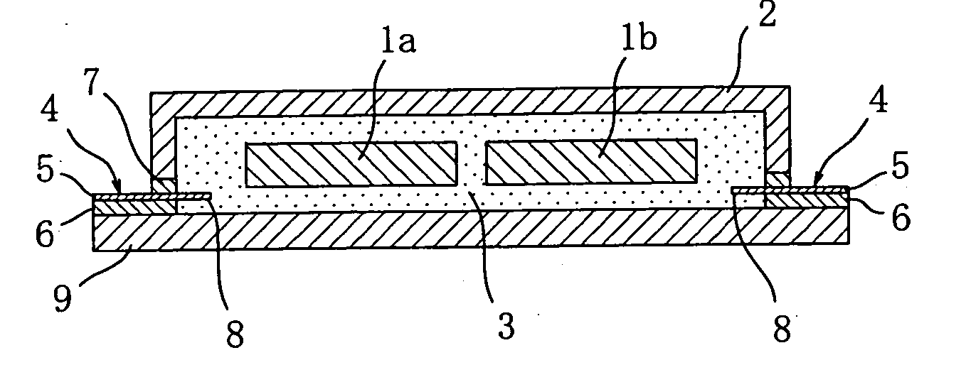
[0087] --Third Embodiment--

[0088] FIG. 5 is a vertical-sectional view of a high-frequency circuit device according to a third embodiment of the present invention. As shown in FIG. 5, the high-frequency circuit device of this embodiment includes a shielding conductor 2 in which two dielectric members 1a, 1b are disposed in series in the longitudinal direction so as to be located at almost the same height. Other parts of the basic structure of the circuit are basically the same as those of the high-frequency circuit device of the first embodiment shown in FIG. 1.

[0089] The high-frequency circuit device of this embodiment can function as a low-loss, two-stage bandpass filter, as has been confirmed in a specific example which will be descried hereinafter.

[0090] --Specific Example of Third Embodiment--

[0091] A high-frequency circuit device having the structure shown in FIG. 5 has been formed in the following manner. As dielectric members 1a, 1b, two dielectric ceramic square poles (forme...

fifth embodiment

[0100] --Fifth Embodiment--

[0101] FIG. 8 is a vertical-sectional view of a high-frequency circuit device according to a fifth embodiment of the present invention. In FIG. 8, a position where a dielectric member 1 is disposed is indicated by a dashed line. In the high-frequency circuit device of this embodiment, a strip conductor 5 and a transmission-line substrate 6 which together form each of transmission lines 4 (microstrip-lines) are buried in a groove formed in a shielding conductor 2 so as to extend in parallel to a shorter side of an earth conductor layer 9, as shown in FIG. 8. More specifically, the strip conductor 5 and the transmission-line substrate 6 are inserted into the groove of the earth conductor layer 9 so as to be located directly under each of end portions of the dielectric member 1. An end portion of the strip conductor 5 faces the underside surface of the dielectric member 1. Moreover, in this embodiment, an end portion 10 of the strip conductor 5 is bent throug...

sixth embodiment

[0108] Sixth Embodiment--

[0109] FIG. 10 is a cross-sectional view of a high-frequency circuit device according to a sixth embodiment of the present invention. The high-frequency circuit device of this embodiment has a structure in which two dielectric members 1a, 1b are disposed in series in the longitudinal direction so as to be located at almost the same height in a shielding conductor 2 as in the third embodiment. Also, a strip conductor 5 is bent through 90 degrees on the transmission-line substrate 6 to form an L shape as in the sixth embodiment. The basic structure for other parts of the high-frequency circuit device of this embodiment is basically the same as that in the fifth embodiment shown in FIG. 8.

[0110] The high-frequency circuit device of this embodiment can function as a low-loss, two-stage bandpass filter, as has been confirmed in a specific example which will be descried hereinafter.

[0111] With the circuit of this embodiment, if the coupling structure of the fifth ...


PUM


Abstract

A high-frequency circuit device includes a dielectric member 1, a shielding conductor 2 surrounding the dielectric member 1, a support member 3 for fixing and supporting the dielectric member 1, and a pair of transmission lines 4 each of which is formed of a microstrip-line. Each of the transmission lines includes a substrate 6 formed of a dielectric material, a strip conductor 5, and an earth conductor layer 9. An end portion of the strip conductor 5 faces part of the dielectric member 1 and functions as a coupling probe for input/output coupling. Each of the transmission lines 4 is formed of a strip line, a mictostrip line, a coplanar line or the like, and has low-loss when connected to a circuit board.

Description

[0001] The present invention relates to high-frequency circuit devices and modules for resonance used in radio-communication systems or other devices dealing with high-frequency signals.[0002] Conventionally, high-frequency filters and other high-frequency circuit devices including a resonant body as a basic element are essential for communication systems. With a resonant body, among resonator bodies, using a dielectric material such as a high dielectric constant, low-loss ceramic material, a high-frequency circuit device functioning as a small and low-loss (high-Q) resonator can be achieved.[0003] Such a resonator can be disposed with other circuit elements such as an amplifier, an oscillator, and a mixer circuit on a substrate to make a high-frequency circuit have a module configuration. In this case, a high-frequency signal needs to be input / output to / from the resonator via a transmission line such as a stripline on the substrate. As an example of such high-frequency circuits usi...

Claims


Application Information

Patent Timeline
IPC IPC(8): H01P1/203H01P1/208H01P1/213H01P7/10
CPCH01P1/20318H01P1/2084H01P7/10H01P1/2138H01P1/2135H01P1/213
Inventor ENOKIHARA, AKIRANAMBA, HIDEKINAKAMURA, TOSHIAKI
Owner PANASONIC CORP
Why Eureka
Try Eureka