Electrostatic discharge protection device and method using depletion switch

Inactive Publication Date: 2004-06-03
TRANSPACIFIC IP LTD
View PDF52 Cites 1 Cited by
  • Summary
  • Abstract
  • Description
  • Claims
  • Application Information

AI Technical Summary

Benefits of technology

0012] To achieve these and other advantages, and in accordance with the purpose of the invention as embodied and broadly described, there is provided an integrated circuit device for electrostatic discharge protection that includes a semiconductor substrate, a lightly doped region of a first dopant type formed in the substrate, a first diffusion region of the first dopant type formed at least partially in the lightly doped region, a second diffusion region of the first dopant type formed a

Problems solved by technology

A semiconductor integrated circuit ("IC") is generally susceptible to an electrostatic discharge ("ESD") event, which may damage or destroy the IC, such as advanced MOSFET transistors.
An IC is susceptible to the HBM and MM during transportation or handling.
For ultra thin gate oxides with such breakdown vol

Method used


Image

  • Electrostatic discharge protection device and method using depletion switch
  • Electrostatic discharge protection device and method using depletion switch
  • Electrostatic discharge protection device and method using depletion switch

Examples


Embodiment Construction

[0036] Reference will now be made in detail to exemplary embodiments of the invention, examples of which are illustrated in the accompanying drawings. Wherever possible, the same reference numbers will be used throughout the drawings to refer to the same or like parts.

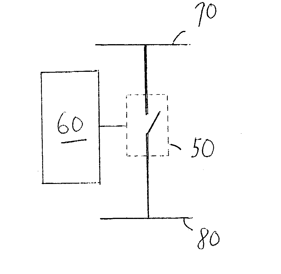
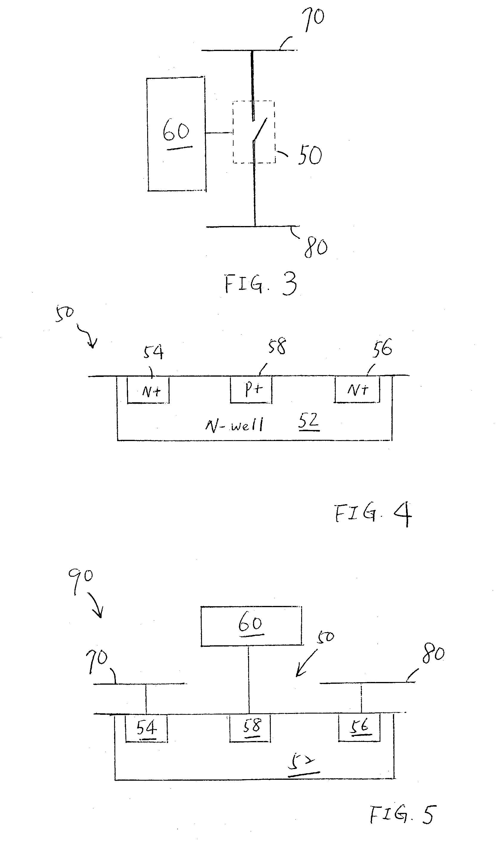
[0037] FIG. 3 shows a schematic view of a depletion switch 50 consistent with an exemplary embodiment of the present invention. As used herein, "depletion switch" means an integrated circuit device in which a resistive path is kept at a low resistive state between two terminals to allow for an ESD current to be conducted through the low resistive path as an ESD event occurs, and in which a depletion region is induced to change the resistive path to a high resistive state as a normal operation period occurs. As also used herein, "normal operation period" means a period during which no ESD events occur. The depletion region induced in a normal operation period is not removed until another ESD event occurs.

[0038] Referrin...


PUM


Abstract

An integrated circuit device for electrostatic discharge protection that includes a semiconductor substrate, a lightly doped region of a first dopant type formed in the substrate, a first diffusion region of the first dopant type formed at least partially in the lightly doped region, a second diffusion region of the first dopant type formed at least partially in the lightly doped region and spaced apart from the first diffusion region, a resistive path defined by the lightly doped region, the first and the second diffusion regions, and a third diffusion region of a second dopant type formed in the lightly doped region, and disposed between and spaced apart from the first and the second diffusion regions, wherein the third diffusion region keeps the resistive path at a low resistive state until a normal operation period occurs.

Description

DESCRIPTION[0001] 1. Related Field[0002] This invention pertains in general to a semiconductor device and, more particularly, to an electrostatic discharge protection device using a depletion switch and a method thereof.[0003] 2. Background of the Invention[0004] A semiconductor integrated circuit ("IC") is generally susceptible to an electrostatic discharge ("ESD") event, which may damage or destroy the IC, such as advanced MOSFET transistors. An ESD event is an electrical discharge of a current (positive or negative) for a short duration during which a large amount of current is provided to the IC. The high current may be built-up from a variety of sources, such as the human body and machines, referred to as the human body model (HBM) and machine model (MM), respectively. An IC is susceptible to the HBM and MM during transportation or handling.[0005] Advanced MOSFET transistors, such as those manufactured using sub-quarter-micron processes, have traditionally required certain prop...

Claims


Application Information

Patent Timeline
IPC IPC(8): H01L23/58H01L27/02H02H9/00
CPCH01L27/0251H01L2924/0002H01L2924/00
Inventor CHANG, CHYH-YIHJIANG, HSIN-CHINKER, MING-DOU
Owner TRANSPACIFIC IP LTD
Why Eureka
Try Eureka