Resistance variable oxide material Co3O4 thin film, preparation and use thereof
An oxide and thin film technology, applied in the field of microelectronic materials, can solve the problems of poor reliability, not yet used in large quantities, and difficult to further improve the recording density, and achieve the effect of uniform thickness
- Summary
- Abstract
- Description
- Claims
- Application Information
AI Technical Summary
Problems solved by technology
Method used
Image
Examples
Embodiment 1
[0043] Example 1. Preparation of CoO x (0x Ceramic target.
Embodiment 2
[0044] Example 2. Preparation of polycrystalline Co 3 o 4 Thin film, its preparation steps are as follows:
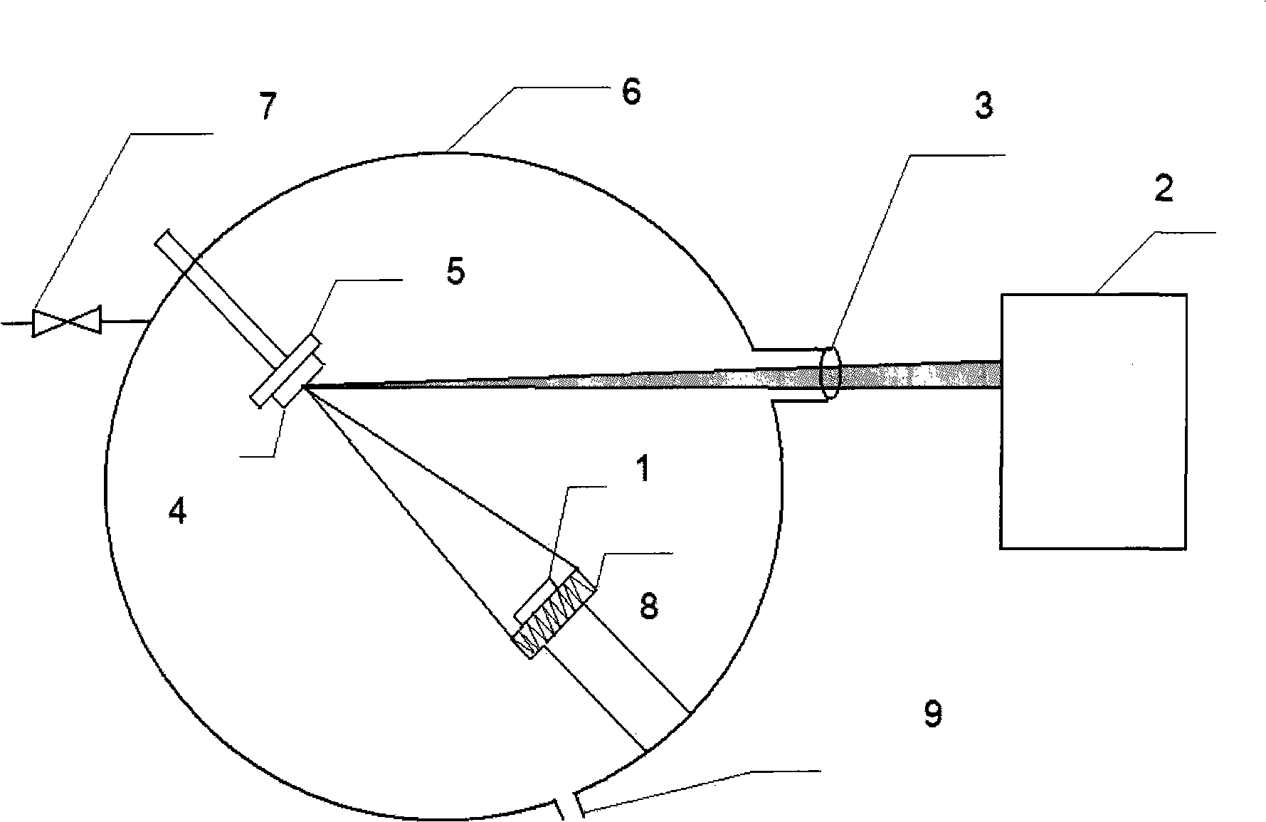
[0045] a) The sintered CoO x The target 4 is fixed in a pulsed laser deposition film forming system (such as figure 1 Shown) on the target stage 5, the substrate 1 is fixed on the substrate stage 8, and they are all located in the growth chamber 6 of the pulsed laser deposition film forming system;
[0046] b) sequentially use a mechanical pump and a molecular pump to vacuum the growth chamber 6 to about 8.0×10 -4 Pa. After turning off the molecular pump, open the needle inlet valve to feed oxygen into the growth chamber. Adjust the oxygen pressure in the growth chamber to 20Pa by adjusting the intake valve.
[0047] c) Start the KrF excimer laser 2 to focus the laser beam on the CoO through the focusing lens 3 x on target 4;
[0048] d) Heating the substrate table with a resistance furnace, Pt / Ti / SiO 2 / Si(111) substrate temperature reaches the set temperature...
Embodiment 3
[0050] Example 3. Using variable Co 3 o 4 A method for preparing a resistive memory element from a thin film, the preparation steps are as follows:
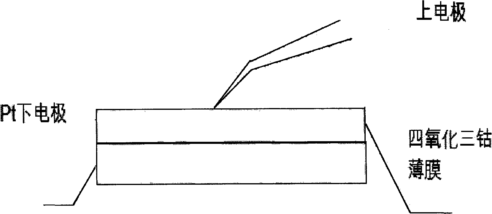
[0051] On Pt / Ti / SiO 2 / Si(111) substrate with a thickness of about 200 nm of Co 3 o 4 Thin film, during the deposition process, press a corner with a press clip, so that the leaked part of the Pt lower electrode film is used as the lower electrode. After taking it out, put it on the probe station, and carefully probe the upper electrode through the auxiliary microscope of the probe station. Ride on Co 3 o 4 On the film, a miniature sandwich structure is formed, which is a memory unit.
PUM
 Abstract
Description
Claims
Application Information


