Apparatuses and methods for forming a substantially facet-free epitaxial film

a substantially facet-free, epitaxial film technology, applied in the direction of chemistry apparatus and processes, single crystal growth, semiconductor devices, etc., can solve the problems of difficult control of the implantation process, further reducing the available surface for device fabrication, and extremely small surface available for device fabrication

Inactive Publication Date: 2004-09-09
APPLIED MATERIALS INC
View PDF33 Cites 169 Cited by
  • Summary
  • Abstract
  • Description
  • Claims
  • Application Information

AI Technical Summary

Problems solved by technology

Selective deposition methods used to form epitaxial film, such as the epitaxial silicon, typically causes faceting.
As devices are scaled to deep submicron regime, (e.g., less than about 0.12 microns) the surfaces available for fabrication of the devices are getting extremely small.
Faceting not only further reduces the available surface for fabrication of the devices, but also causes other problems.
Faceting causes unevenness in the surface which makes it difficult to control the implantation process including controlling the consistency of ions implantation across the epitaxial regions.
Another problem is that one needs to modify the deposition process for the epitaxial regions depending on the amount of the opening windows (exposed substrate) where the epitaxial regions are formed.
Such need for modification makes it even more difficult to control consistence thickness for the epitaxial regions from one substrate or one wafer to another.

Method used


Image

  • Apparatuses and methods for forming a substantially facet-free epitaxial film
  • Apparatuses and methods for forming a substantially facet-free epitaxial film
  • Apparatuses and methods for forming a substantially facet-free epitaxial film

Examples


Embodiment Construction

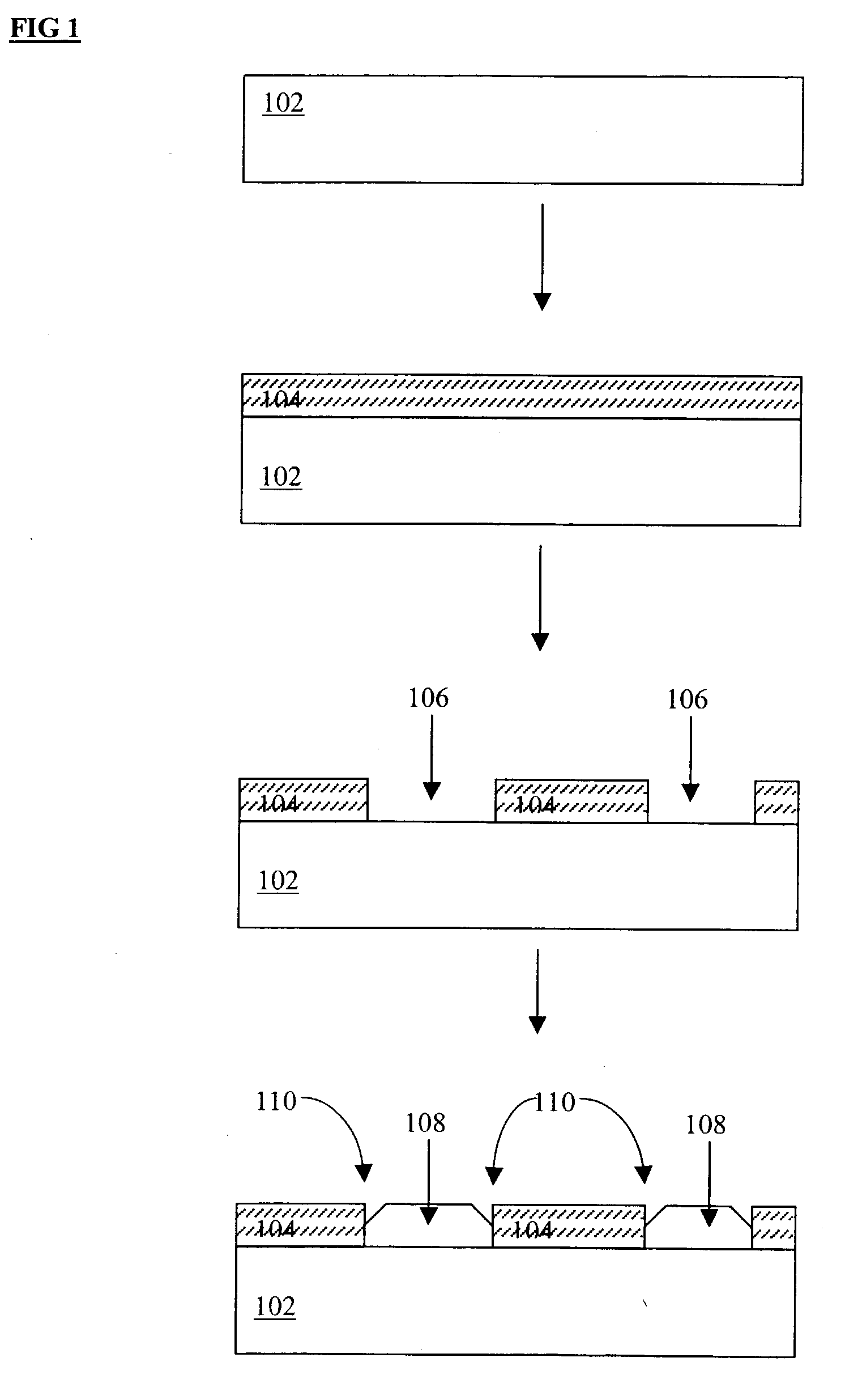
[0021] The present invention describes methods and apparatuses for selectively deposing an epitaxial film that is substantially facet-free. In the following description numerous specific details are set forth in order to provide a thorough understanding of the present invention. One skilled in the art will appreciate that these specific details are not necessary in order to practice the present invention. In other instances, well known equipment features and processes have not been set forth in detail in order to not unnecessarily obscure the present invention.

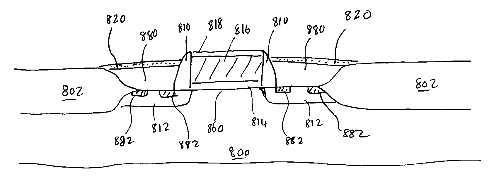
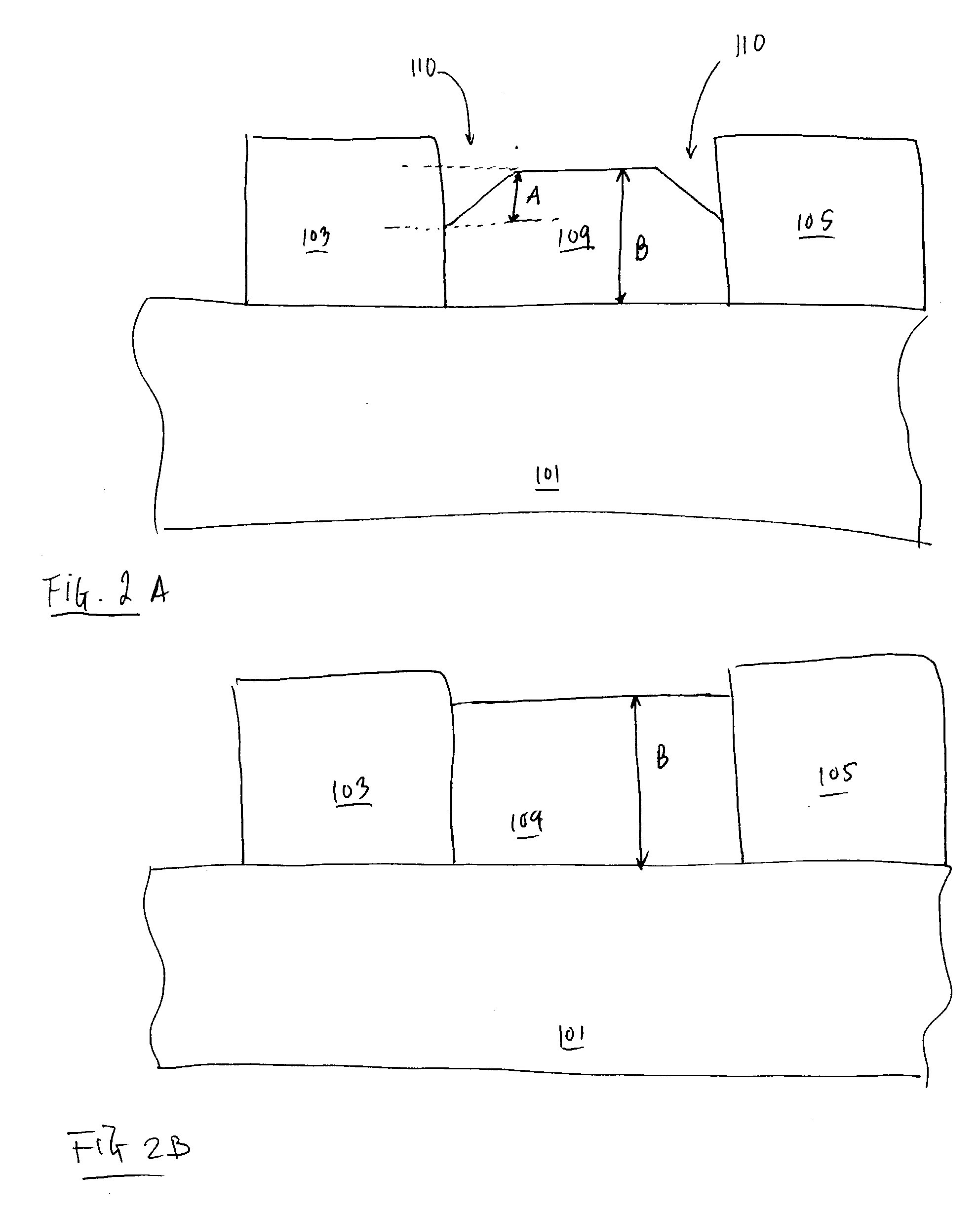
[0022] As mentioned above, faceting is the formation of another growth plane at a different angle from the major surface of the epitaxial silicon regions and often, at the sides of the regions that meet the wall of the structures already formed on the substrate. See for example, facets 110 illustrated in FIG. 1. Thus, the plane of the facet is along a different crystallographic plane than the major surface of the epitaxial fil...


PUM

PropertyMeasurementUnit
temperatureaaaaaaaaaa

Abstract

A method of making a substantially facet-free epitaxial film is disclosed. A substrate having predetermined regions is first provided. An epitaxial film forming process gas and a carrier gas are introduced into a reactor chamber. The epitaxial film forming process gas and the carrier have a flow ratio between 1:1 and 1:200. The epitaxial film is deposited into the predetermined regions of the substrate wherein the substrate has a temperature between about 350° C. and about 900° C. when the epitaxial film is being deposited.

Description

[0001] 1. FIELD OF THE INVENTION[0002] The present invention relates to apparatus and method of forming a substantially facet-free epitaxial film.[0003] 2. DISCUSSION OF RELATED ART[0004] Selective deposition is used in many applications of semiconductor fabrication. For example, selective epitaxial film deposition is used to form isolated regions for semiconductor devices, raised or elevated source / drain regions, heterojunctions bipolar transistors, and ultra shallow junctions, to name a few.[0005] An epitaxial film is typically made of a semiconductor material such as silicon, germanium, silicon alloy, or germanium alloy. A common epitaxial film is epitaxial silicon. An epitaxial silicon film, or rather, regions, can be selectively formed or deposited on a substrate having patterns already incorporated therein. For example, the substrate may include patterns such as gate electrodes, spacers, oxide films, or other structures formed thereon. In one example, and as illustrated in FIG...

Claims


Application Information

Patent Timeline
Patent Type & Authority Applications(United States)
IPC IPC(8): C30B25/02H01L21/00H01L21/20H01L21/205H01L21/28H01L21/336
CPCH01L21/02639H01L21/02381H01L21/0262H01L21/02576H01L21/02579H01L21/02532
Inventor VATUS, JEAN R.SCUDDER, LANCE A.COMITA, PAUL B.
Owner APPLIED MATERIALS INC
Why Eureka
Try Eureka