On-chip scan clock generator for asic testing

a technology of asic testing and scan clock, which is applied in the direction of electronic circuit testing, measurement devices, instruments, etc., can solve the problems of timing violation in scan test mode and may be overlooked

Inactive Publication Date: 2004-09-30
AVAGO TECH WIRELESS IP SINGAPORE PTE
View PDF5 Cites 80 Cited by
  • Summary
  • Abstract
  • Description
  • Claims
  • Application Information

AI Technical Summary

Problems solved by technology

The scan clock signal may differ substantially from the functional mode clock signals at each flip flop, resulting in possible timing violations in the scan test mode which would not occur in the functional mode.
These timing violations may be overlooked due to a lack of understanding of the differences between functional mode clocking versus scan clocking.

Method used


Image

  • On-chip scan clock generator for asic testing
  • On-chip scan clock generator for asic testing
  • On-chip scan clock generator for asic testing

Examples


Embodiment Construction

[0013] The present invention is illustrated by way of example and not limitation in the accompanying figures, in which like references indicate similar elements throughout the several views of the drawings, and in which:

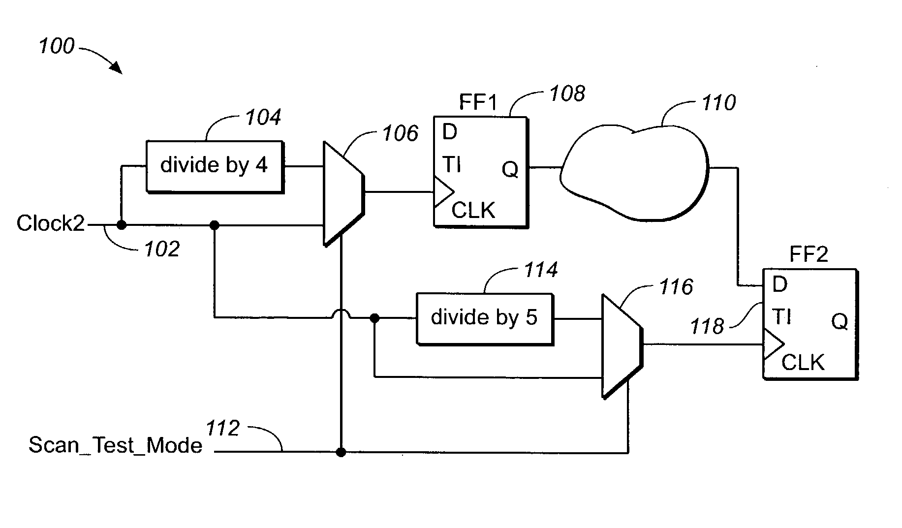
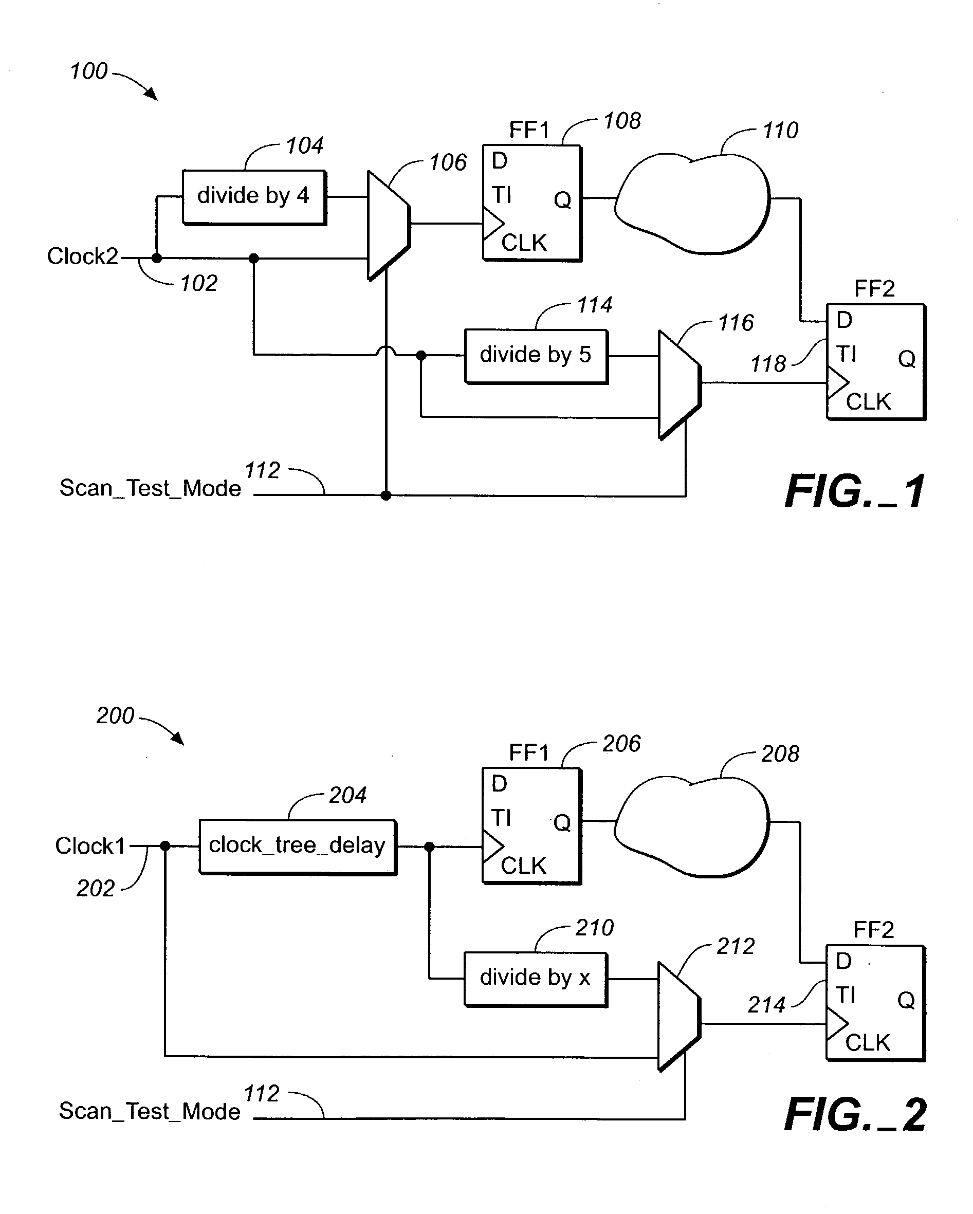
[0014] FIG. 1 illustrates an example of a scan test circuit of the prior art that creates a new timing path;

[0015] FIG. 2 illustrates an example of a scan test circuit of the prior art that disregards clock tree insertion delay;

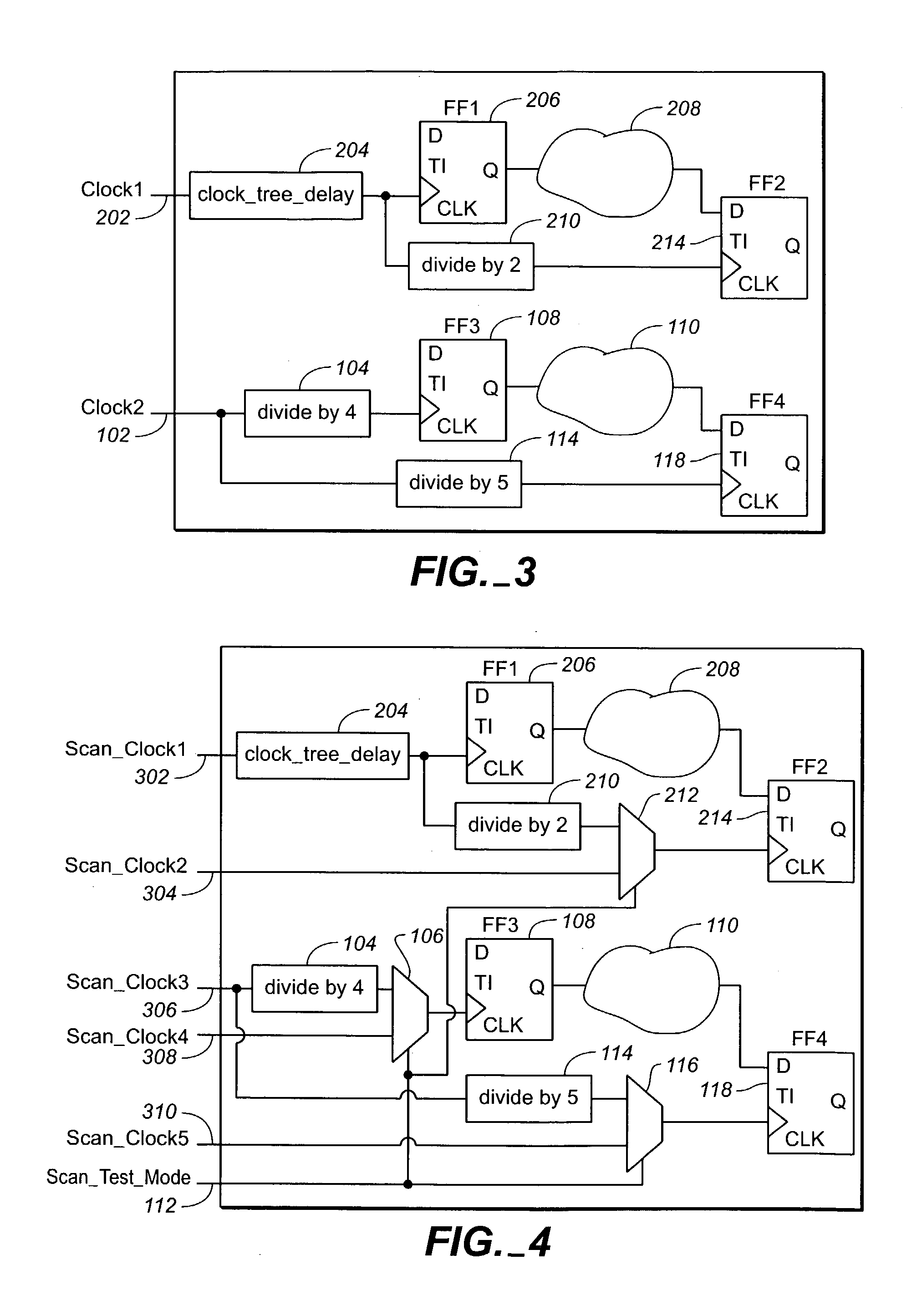
[0016] FIG. 3 illustrates the circuits of FIGS. 1 and 2 before inserting scan test logic;

[0017] FIG. 4 illustrates the circuit of FIG. 3 including scan test logic inserted according to an embodiment of the present invention;

[0018] FIG. 5 illustrates an example of a scan clock generator for the scan test logic of FIG. 4;

[0019] FIG. 6 illustrates an example of a circuit that may be included with the scan clock generator of FIG. 5 for testing chips that require low power consumption;

[0020] FIG. 7 illustrates the integration of a circuit and scan ...


PUM


Abstract

A a clock signal input for receiving a clock signal, a scan shift mode signal input for receiving a scan shift mode signal, and a sequence controller coupled to the clock signal input for gating a selected number of clock signal pulses at a time to generate a sequence of nonconcurrent scan clock signals at separate outputs respectively in response to a first state of the scan shift mode signal.

Description

[0001] 1. Field of the Invention[0002] The present invention is directed to testing application specific integrated circuit (ASIC) designs. More specifically, but without limitation thereto, the present invention is directed to an on-chip scan clock generator for generating multiple scan clock signals during testing of an ASIC design.[0003] 2. Description of the Prior Art[0004] In testing application specific integrated circuit (ASIC) designs, complex clock structures used for the operating or functional mode of the ASIC must be simplified for scan test mode, for example, by multiplexing the functional mode clock signals with the scan clock signal so that the clock inputs of all flip flops in the ASIC may be accessed from the available input pins of the ASIC. The term "flip flop" is used herein to include all types of devices in an integrated circuit that have a clocked input, including but not limited to memory circuits. The scan clock signal may differ substantially from the funct...

Claims


Application Information

Patent Timeline
Patent Type & Authority Applications(United States)
IPC IPC(8): G01R31/3185
CPCG01R31/318552
Inventor CLARK, IAINDIRKS, JUERGEN
Owner AVAGO TECH WIRELESS IP SINGAPORE PTE
Why Eureka
Try Eureka