Redistribution layer shielding of a circuit element

a circuit element and shielding technology, applied in the field of integrated circuits, can solve the problems of inductors inside the pll, inductors susceptible to electromagnetic interference, and difficult to achieve such a high-q with conventional on-chip inductors,

Inactive Publication Date: 2004-11-11
SILICON LAB INC
View PDF30 Cites 54 Cited by
  • Summary
  • Abstract
  • Description
  • Claims
  • Application Information

AI Technical Summary

Problems solved by technology

It is difficult to achieve such a high-Q with conventional on-chip inductors using conductor and dielectric layer compositions and thicknesses which are typically encountered in traditional integrated circuit processes.
In addition, such inductors are susceptible to electromagnetic interference from external sources of noise.
Inductors inside of the PLL, particularly inside an LC oscillator included in the PLL, are most prone to pulling.

Method used


Image

  • Redistribution layer shielding of a circuit element
  • Redistribution layer shielding of a circuit element
  • Redistribution layer shielding of a circuit element

Examples


Embodiment Construction

)

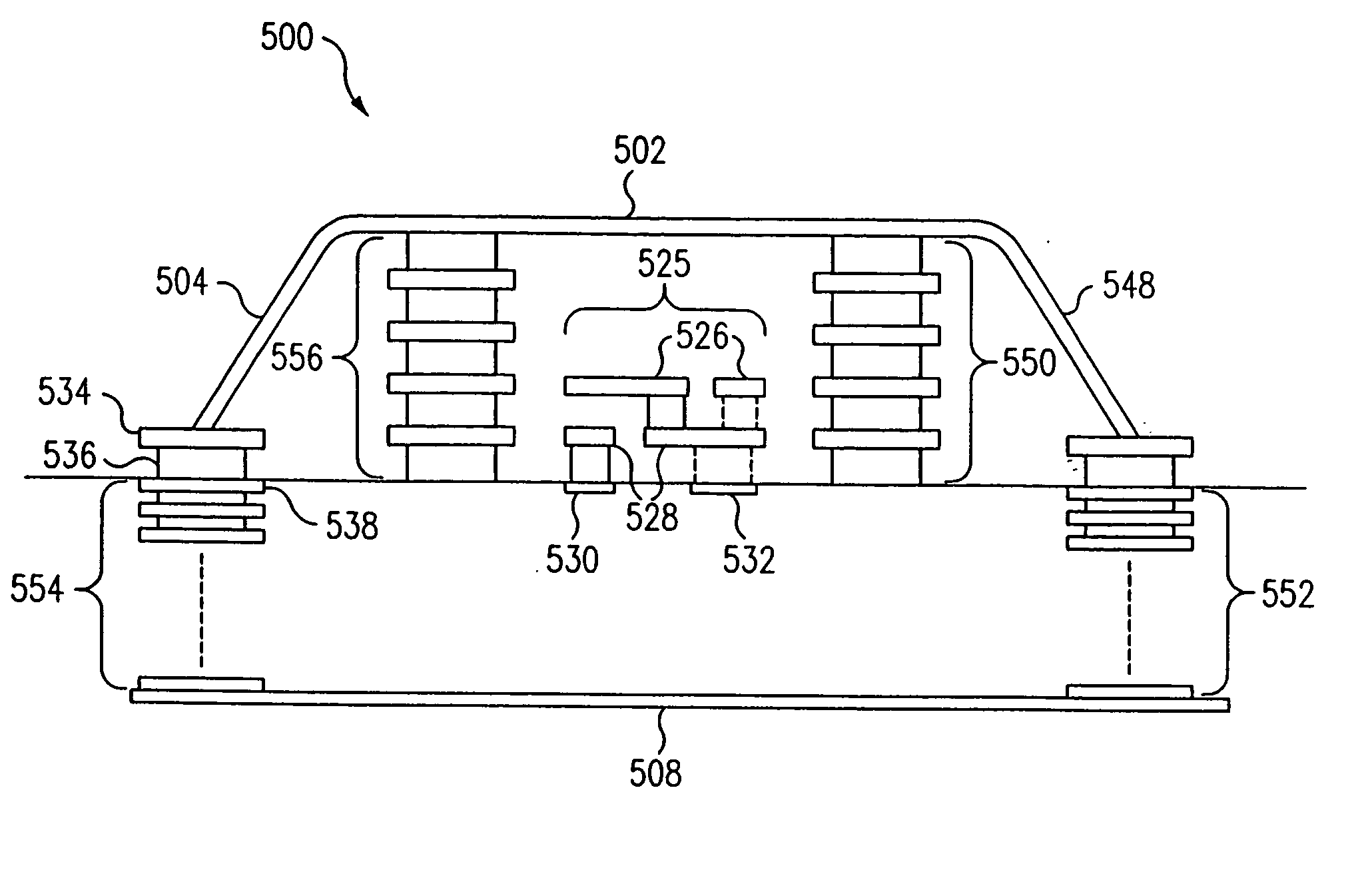
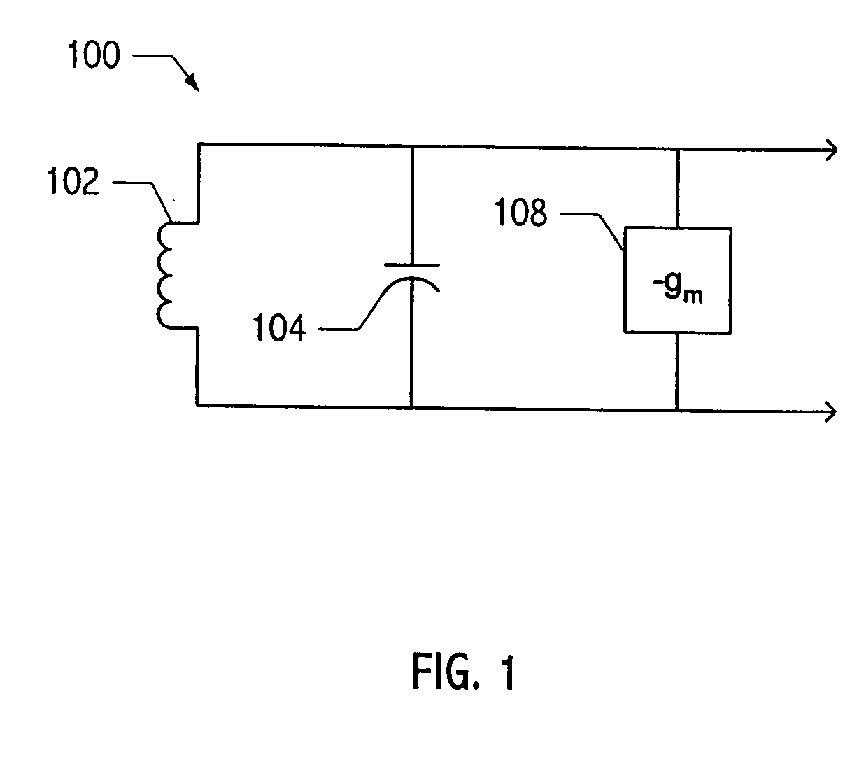
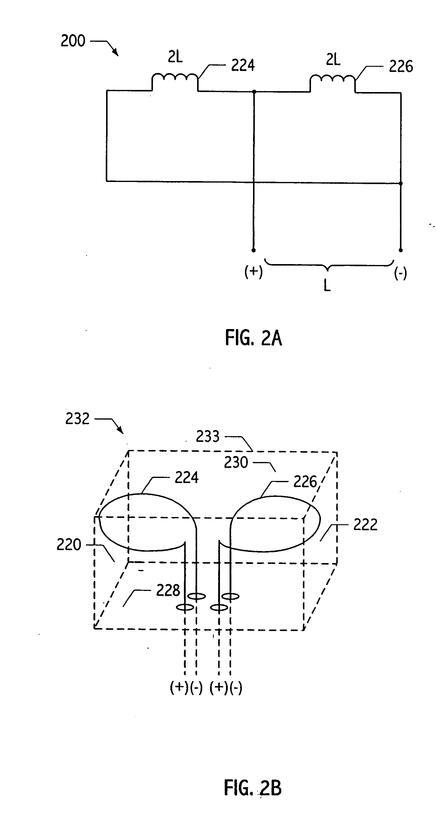
[0040] Referring to FIG. 1, an integrated circuit die includes an LC oscillator circuit e.g., circuit 100, including inductor 102, capacitor 104, and gain stage 108. The Q (i.e., quality factor) associated with the resonant circuit describes the ability of the circuit to produce a large output at a resonant frequency and also describes the selectivity of the circuit. The Q of a resonant circuit is inversely related to interference from outside sources. One way to reduce electromagnetic interference affecting an inductor structure includes implementing the inductor structure as a two-loop arrangement. Circuit 200 of FIG. 2A, illustrates two parallel-connected inductor coils (e.g., loops 224 and 226), and circuit 250 of FIG. 2C, illustrates two series-connected inductor coils (e.g., loops 264 and 266). These two-loop arrangements are less susceptible to external electromagnetic interference (e.g., far field interference sources in particular) because induced current flow in one such ...


PUM


Abstract

In some embodiments of the present invention, an apparatus includes an electromagnetic shielding structure. The electromagnetic shielding structure is formed at least partially in one or more redistribution layers formed on an integrated circuit die. The electromagnetic shielding structure substantially surrounds a circuit element, such as an inductor structure. The circuit element may be formed at least partially in the one or more redistribution layers. An inductor structure may be constructed as a loop structure at least partially in one or more redistribution layers formed on the integrated circuit die. The shielding structure may be formed at least partially in one or more redistribution layers of the integrated circuit die to enclose the inductor in a Faraday cage-like enclosure. The redistribution layers may be formed above integrated circuit pads or above a passivation layer of the integrated circuit die.

Description

CROSS-REFERENCE TO RELATED APPLICATION(S)[0001] This application is a continuation-in-part of co-pending application Ser. No. 10 / 463,961, filed Jun. 18, 2003, entitled "Integrated Circuit Package Configuration Incorporating Shielded Circuit Element Structure," naming Derrick C. Wei, Ying Shi, Kevin G. Smith, Steven P. Proffitt, Axel Thomsen, David Pietruszynski, and Ligang Zhang as inventors, which claims the benefit under 35 U.S.C. .sctn. 119(e) of U.S. Provisional Application No. 60 / 418,546, filed Oct. 15, 2002, entitled "Integrated Circuit Package Configuration Incorporating Shielded Inductor Structure," naming Derrick C. Wei, Ying Shi, Kevin G. Smith, Steven P. Proffitt, Axel Thomsen, and David Pietruszynski as inventors, which applications are incorporated herein by reference.[0002] 1. Field of the Invention[0003] The present invention relates to integrated circuits, and more particularly to such integrated circuits incorporating shielded inductor structures.[0004] 2. Descripti...

Claims


Application Information

Patent Timeline
Patent Type & Authority Applications(United States)
IPC IPC(8): H01L23/552H01L23/64
CPCH01F2017/008H01L23/552H01L23/645H01L2224/16H01L2924/01079H01L2924/15311H01L2924/3025H01L2224/16225H01L2924/00014H01L2224/0401
Inventor ZHANG, LIGANGELDREDGE, ADAM B.THOMSEN, AXELMISRA, ABHAY
Owner SILICON LAB INC
Why Eureka
Try Eureka