

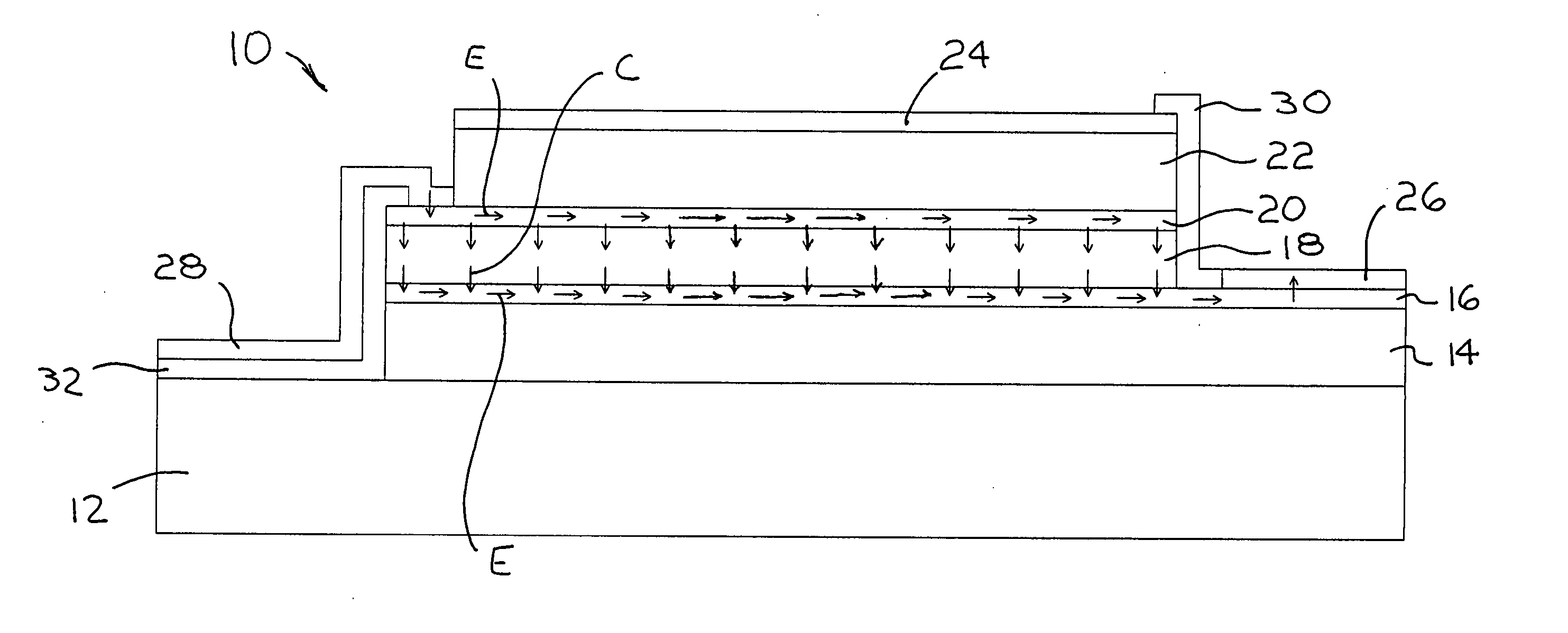
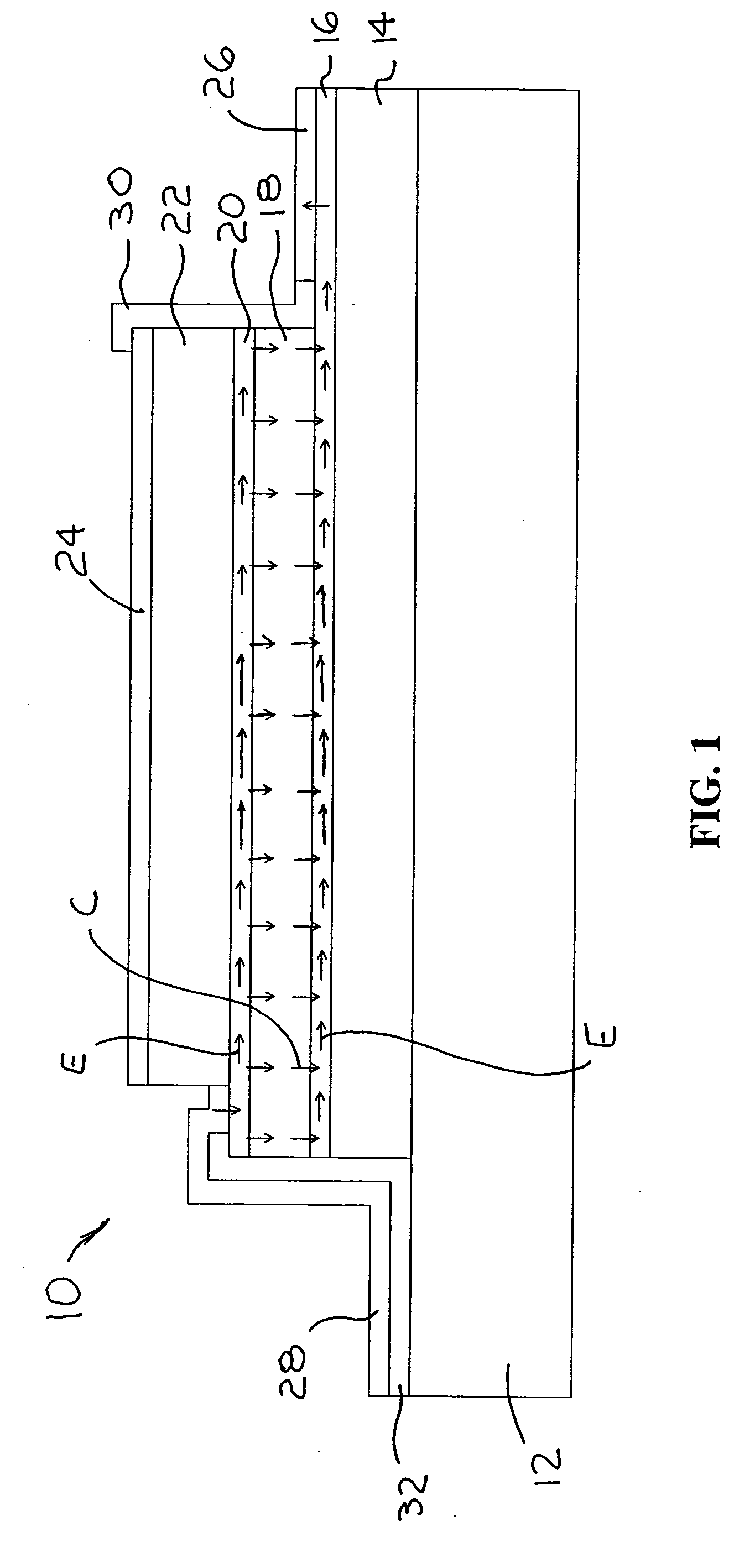
Semiconductor light emitting devices including embedded curent injection layers
a technology of semiconductor light emitting devices and current injection layers, which is applied in the direction of semiconductor devices, lasers, semiconductor lasers, etc., can solve the problems of compromising the optical characteristics of the optical carrier, significant voltage drops and free-carrier optical loss, and the inability to conduct electric current usually tends to decreas
- Summary
- Abstract
- Description
- Claims
- Application Information
AI Technical Summary
Problems solved by technology
Method used
Image

Examples
example 2
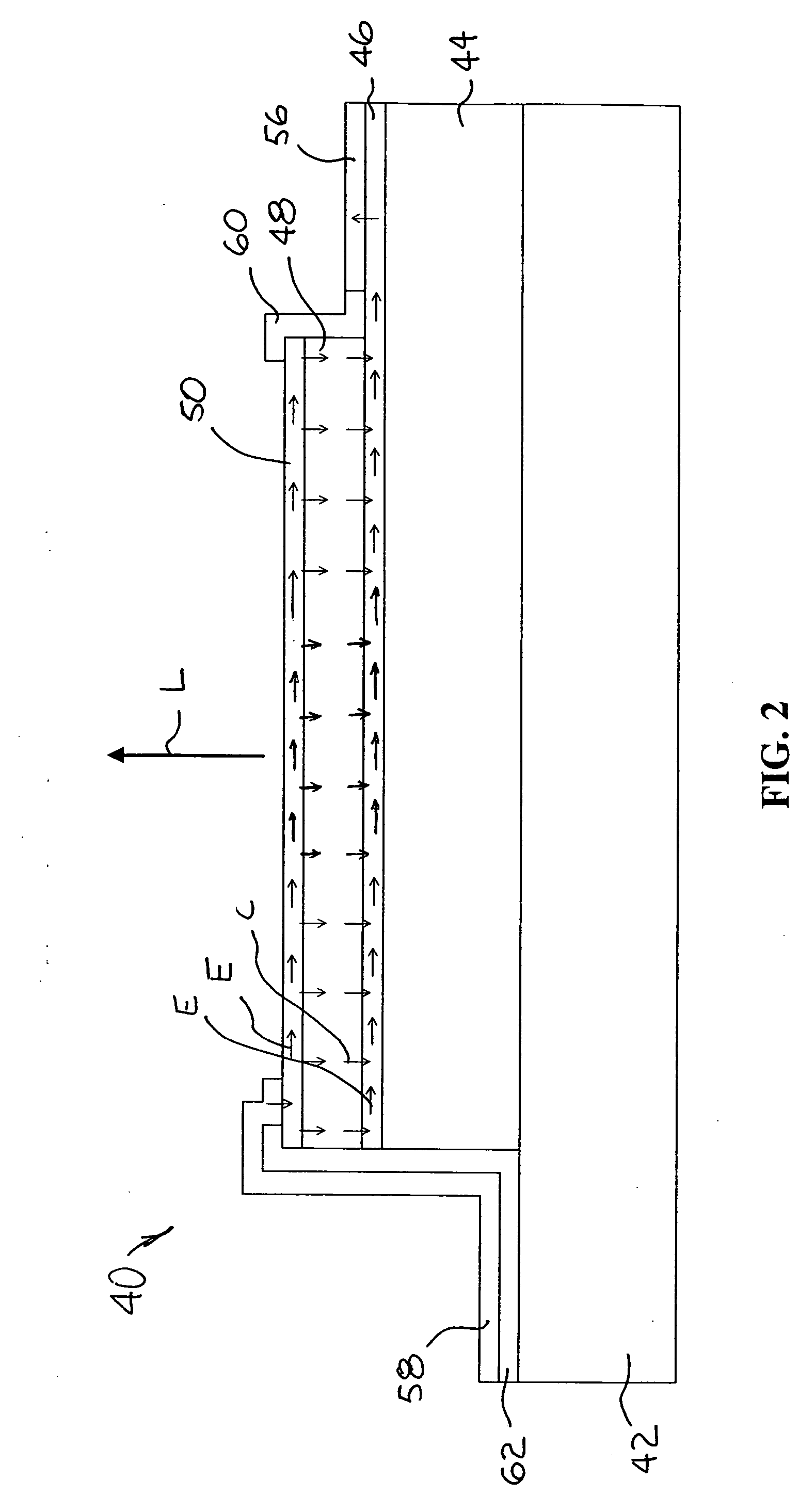
[0038] Example 1 was repeated, except the lateral injection layer Be doping was decreased to 4.times.10.sup.18 cm.sup.-3. The operating characteristics of lasers fabricated from this material showed that this version of the lateral current injection layer worked well for current injection. Devices made from this material lased.
example 3
[0039] Example 1 was repeated, except the lateral injection layer thickness was decreased to 0.3 .mu.m. Once again, the operating characteristics of lasers fabricated from this material showed that this version of the lateral current injection layer worked well for current injection. Overall, lasers fabricated from this material worked well.
example 4
[0040] Example 3 was repeated, except the AlAsSb ternary cladding material was replaced with an AlSb / AlAs cladding superlattice. The lateral injection again worked well, and the overall laser performance was good.
PUM
 Abstract
Description
Claims
Application Information