Substrate processing apparatus and substrate processing method

a substrate processing and substrate technology, applied in the manufacturing of semiconductor/solid-state devices, electrical equipment, basic electric elements, etc., can solve the problems of reducing the uniformity of film thickness and possible yield loss of conventional substrate processing methods

Inactive Publication Date: 2004-12-16
TOKYO ELECTRON LTD
View PDF7 Cites 17 Cited by
  • Summary
  • Abstract
  • Description
  • Claims
  • Application Information

AI Technical Summary

Benefits of technology

[0015] Also, a substrate processing apparatus according to the present invention preferably comprises a top plate which is placed in proximity to the front-side surface of said substrate, said top plate relatively moving to a position close to the front-side surface of said substrate and to a position far from the front-side surface of said substrate. In this case, the temperatures of a processing liquid and the front-side surface of the substrate can be maintained at favorable levels since the atmospheric effects from above the substrate is inhibited. Furthermore, a substrate processing apparatus according to the present invention can comprise a gas feeder for feeding a temperature-controlled gas to the periphery of said substrate. In this case, the temperature around the substrate can be regulated.
[0031] A substrate processing method according to the present invention can also be characterized by forming a liquid film of the processing liquid on the front-side surface of said substrate. In addition, rotating said substrate is preferable in processing by feeding the processing liquid to the front-side surface of said substrate. In this case, pooling of the processing liquid is prevented, and thereby processing of the substrate can be uniformly proceeded.

Problems solved by technology

Consequently, watermarks tend to be generated in a case that the wafer or the like proceeds to cleaning processing and drying processing without any other processing in between, which leads to a possible yield loss.
However, the problem is that uniformity of the film thickness would be reduced by the conventional substrate processing method.

Method used


Image

  • Substrate processing apparatus and substrate processing method
  • Substrate processing apparatus and substrate processing method
  • Substrate processing apparatus and substrate processing method

Examples


Embodiment Construction

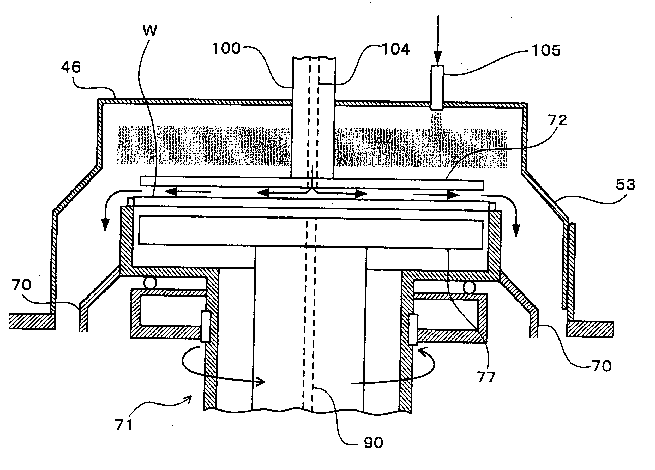
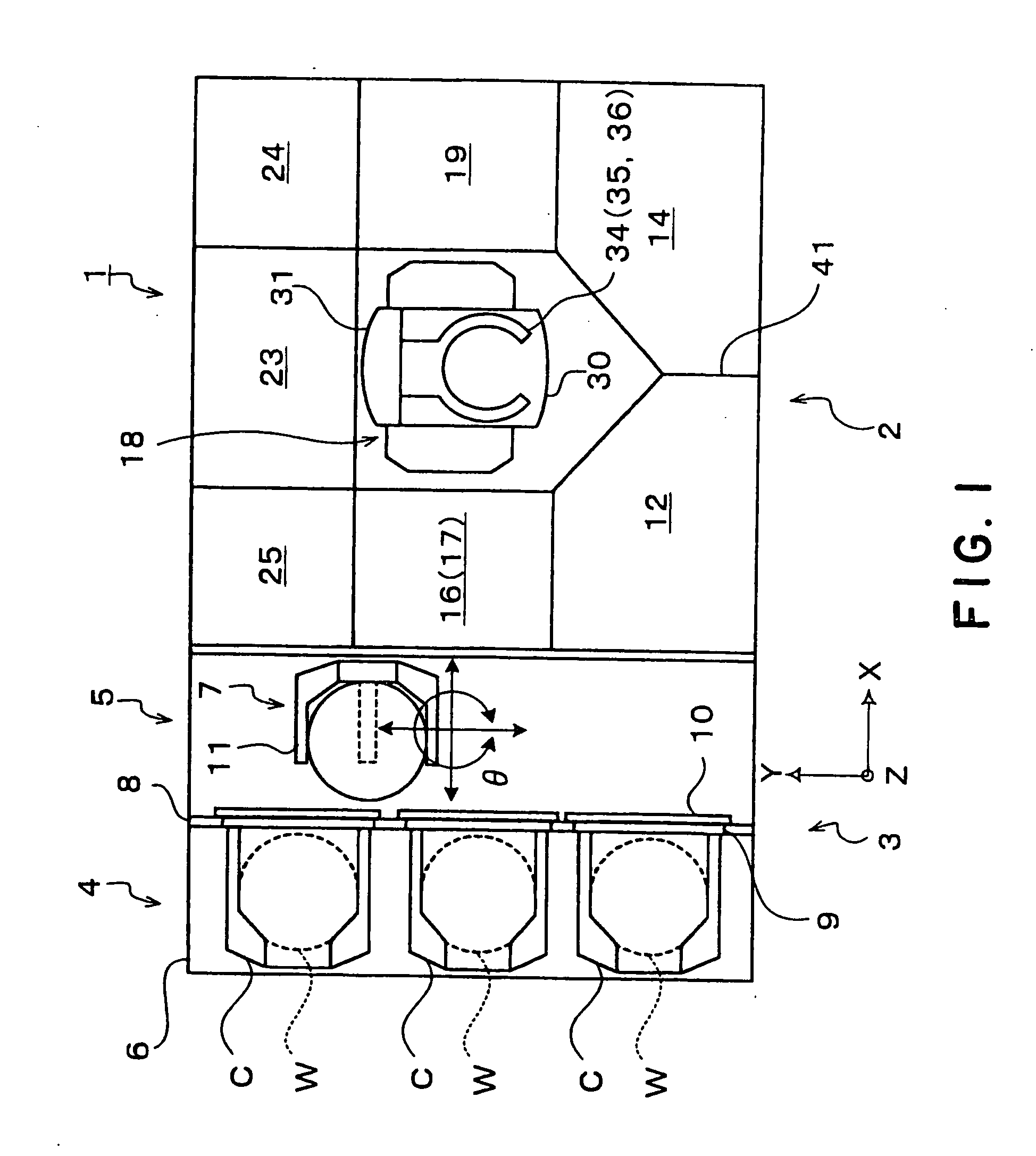
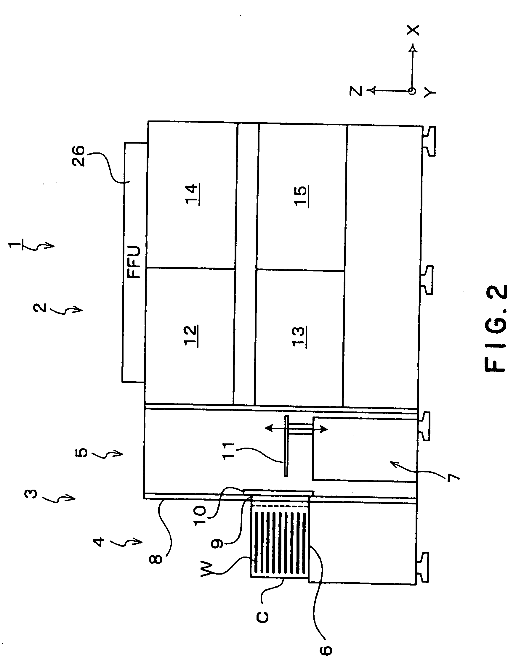
[0047] Preferred embodiments of the present invention will be hereinafter explained based on a substrate-processing unit, as a substrate processing apparatus, structured to conduct processing of the surface of a wafer as an example of a substrate, such as etching and hydrophilization. FIG. 1 is a plane view of the processing system 1 incorporating substrate-processing units 12, 13, 14 and 15 according to the present embodiment. FIG. 2 is a side view of the processing system 1. This processing system 1 comprises: a processing module 2 for thermal processing of a wafer W during and after substrate processing; and a load / unload module 3 to load or unload a wafer W into or from the processing module 2.

[0048] The load / unload module 3 comprises: an in / out port 4 providing a mount stand 6 to mount a holder (carrier C) which can accommodate a plurality of wafers, 25 wafers W for example, at regular intervals in a substantially horizontal position; and a wafer carrying module 5 equipped with...


PUM

PropertyMeasurementUnit
temperatureaaaaaaaaaa
hydrophobicaaaaaaaaaa

Abstract

A substrate processing apparatus and a substrate processing method are provided wherein an oxide film which is thinner than the conventional films can be formed with uniform thickness when forming an oxide film on the front-side surface of a substrate. A substrate processing apparatus (12) for processing a substrate (W) by feeding a processing liquid comprises: a temperature regulator (133) to regulate the temperature of said processing liquid; and a underplate temperature adjuster (115) to adjust the temperature of an underplate (77) which is placed in proximity to the backside surface of said substrate W.

Description

[0001] The present invention relates to a substrate processing apparatus and a substrate processing method for processing the surface of a substrate such as a semiconductor wafer for example.BACKGROUND TECHNOLOGY[0002] Generally, the manufacturing process of a semiconductor device includes a series of processing steps of: applying photoresist to a semiconductor wafer or the like as a substrate-to-be-processed (hereinafter referred to as a "wafer or the like"); printing an image of a circuit pattern on the photoresist; and then removing the photoresist from the wafer or the like.[0003] In the above-mentioned processing, if an oxide film on the surface of a wafer or the like is removed by etching with a chemical liquid, dilute hydrofluoric acid (DHF) for example, the surface of the wafer or the like will become hydrophobic. Consequently, watermarks tend to be generated in a case that the wafer or the like proceeds to cleaning processing and drying processing without any other processi...

Claims


Application Information

Patent Timeline
Patent Type & Authority Applications(United States)
IPC IPC(8): H01L21/00
CPCH01L21/67051H01L21/6708H01L21/67248H01L21/02
Inventor TAKEHIKO, ORIIAMAI, MASARU
Owner TOKYO ELECTRON LTD
Why Eureka
Try Eureka