

Susceptor for epitaxial growth and epitaxial growth method
a technology of epitaxial growth and susceptor, which is applied in the direction of polycrystalline material growth, crystal growth process, chemically reactive gas growth, etc., can solve the problems of reducing the strength of the susceptor itself, slipping, and ineffective exhaustion of the dopant that diffuses outwards from the rear surface of the wafer, so as to reduce the degradation region and improve the uniformity of the concentration of the dopant
Inactive Publication Date: 2005-01-06
SUMITOMO MITSUBISHI SILICON CORP
View PDF6 Cites 55 Cited by
- Summary
- Abstract
- Description
- Claims
- Application Information
AI Technical Summary
Benefits of technology
[0020] It is therefore an object of the present invention to provide an epitaxial growth susceptor and epitaxial growth method capable of providing uniformity with regards to film thickness of an epitaxial film, to reduce degradation regions regarding nanotopography of the surface of an epitaxial wafe
Problems solved by technology
If the total opening surface area of the plurality of through-holes is smaller than 0.05% of the surface area of the bottom wall, dopant that diffuses outwards from the rear surface of the wafer is not effectively exhausted.
Further, when the total opening surface area exceeds 55%, slip
Method used
View moreImage
Smart ImageViewing Examples

Examples
 PUM
| Property | Measurement | Unit |
|---|---|---|
| Fraction | aaaaa | aaaaa |
| Fraction | aaaaa | aaaaa |
| Fraction | aaaaa | aaaaa |
Abstract
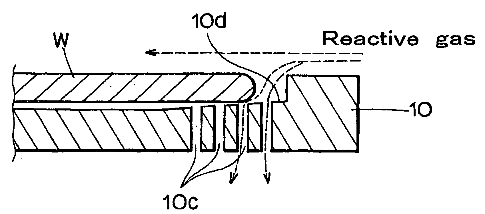
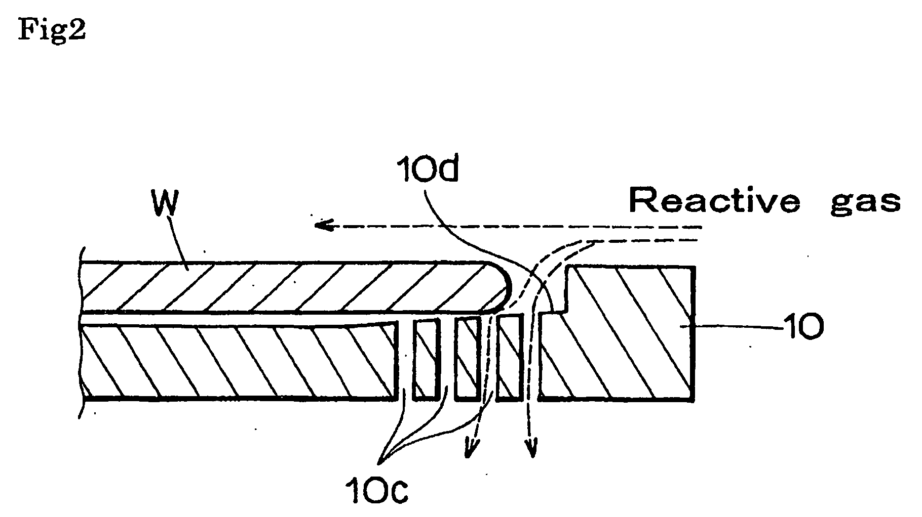
A susceptor for use in an epitaxial growth apparatus and method where a plurality of circular through-holes are formed in the bottom wall of a pocket in an outer peripheral region a distance of up to about ½ the radius toward the center of the circular bottom wall. The total opening surface area of these through-holes is 0.05 to 55% of the surface area of the bottom wall. The opening surface area of each of the through-holes provided at this outer peripheral region is 0.2 to 3.2 mm2 and the density of the through-holes is 0.25 to 25 per cm2. After a semiconductor wafer is mounted in the pocket, epitaxial growth is carried out while source gas and carrier gas (i.e., reactive gas) is made to flow on the upper surface side of the susceptor and carrier gas is made to flow on the lower surface side.
Description
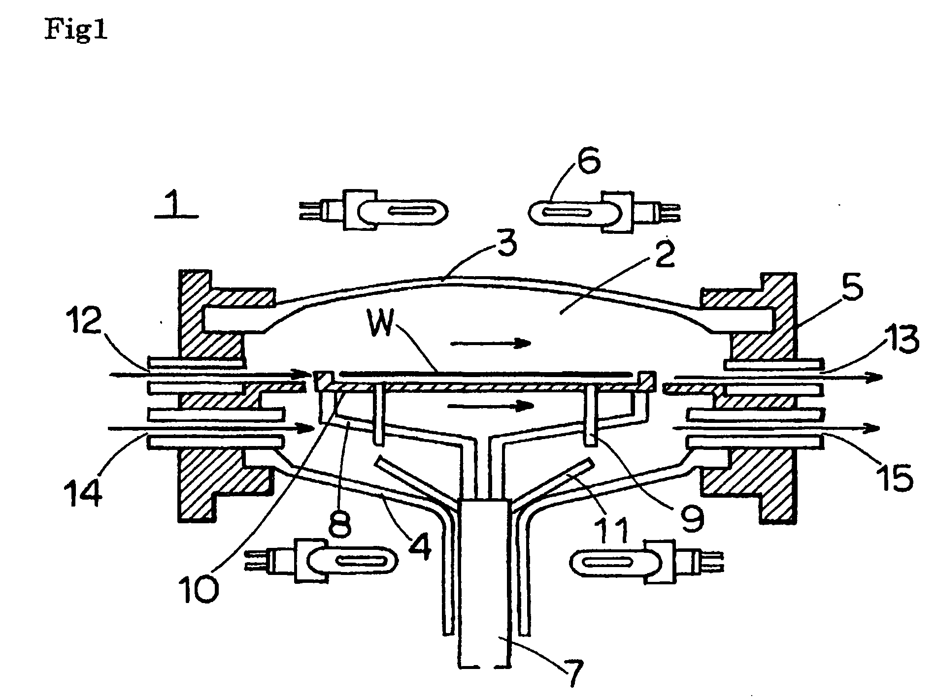
FIELD OF THE INVENTION [0001] This invention relates to a susceptor for epitaxial growth and an epitaxial growth method, and in particular relates to a susceptor for epitaxial growth and epitaxial growth technology for use in promoting growth of an epitaxial film on the surface of a semiconductor wafer. BACKGROUND OF THE INVENTION [0002] In recent years, epitaxial wafers where an epitaxial film is formed on the surface of a silicon wafer are widely used as silicon wafers for use with MOS devices. These epitaxial wafers provide improved yield for gate oxidation films of MOS devices, and have superior characteristics such as the reduction of parasitic capacitance, the prevention of soft errors, improved gettering performance, and improved mechanical strength. [0003] With this epitaxial wafer structure, in the prior art where a batch method is implemented so as to perform epitaxial growth process simultaneously on a plurality of silicon wafers, it has become difficult to maintain compa...
Claims
Login to View More Application Information
Patent Timeline
 IPC IPC(8): C23C16/44C23C16/455C23C16/458C30B25/12C30B29/06H01L21/687
CPCC30B29/06C23C16/4584C23C16/4585C30B25/12C23C16/45519H01L21/68735H01L21/02579H01L21/02532H01L21/0262H01L21/2205H01L21/20C23C14/50C23C14/54H01L21/68785C23C16/4583C23C16/45521H01L21/02381
InventorISHIBASHI, MASAYUKIKRUEGER, JOHN FDOHI, TAKAYUKIHORIE, DAIZOFUJIKAWA, TAKASHI
OwnerSUMITOMO MITSUBISHI SILICON CORP