

Drive method and drive device of a light emitting display panel
- Summary
- Abstract
- Description
- Claims
- Application Information
AI Technical Summary
Benefits of technology
Problems solved by technology
Method used
Image

Examples
first embodiment
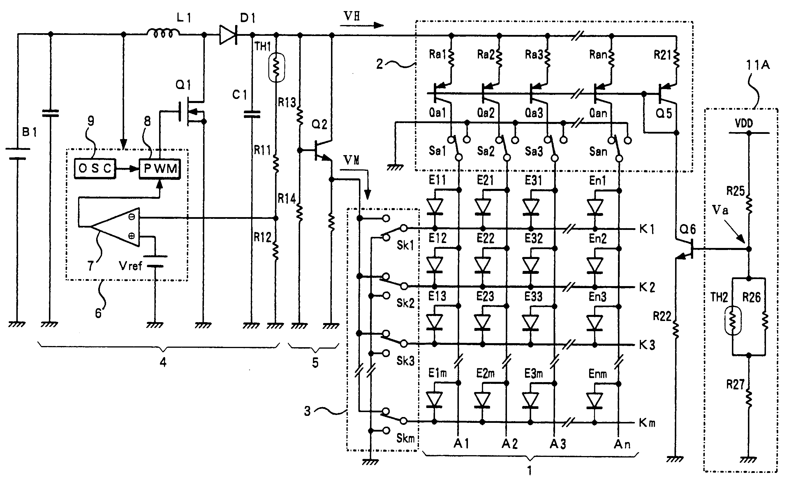
[0054] Preferred embodiments of a drive device of a light emitting display panel according to the present invention will be described below with reference to the drawings. FIG. 7 shows a first embodiment thereof and shows an example applied to a drive device of a passive drive type display panel. In FIG. 7, parts corresponding to the respective constituent elements shown in FIG. 3 already described are designated by the same reference characters and numerals, and therefore detailed explanation thereof will be omitted. In the embodiment shown in this FIG. 7, a thermistor TH1 is equipped as described above in a voltage boosting circuit 4 designated by the reference numeral 4 in a DC / DC converter, and by this, temperature compensation is performed as already described above.
[0055] The temperature compensation operation of this case is operated in such away that EL elements E11 to Enm as light emitting elements are driven to be lit so as to have an approximately constant light emission ...
second embodiment
[0065]FIG. 8 shows a second embodiment in a drive device of a display panel according to the present invention and shows an example applied similarly to a drive device of a passive drive type display panel. FIG. 8 is shown in such a way that the DC / DC converter section and the reverse bias voltage generation circuit 5 in the embodiment shown in FIG. 7 already described are omitted. In FIG. 8, parts corresponding to the respective constituent elements shown in FIG. 7 are designated by the same reference characters and numerals, and therefore detailed explanation thereof will be omitted.
[0066] In the embodiment shown in this FIG. 8, the structure of a temperature detection means 11B is a bit different from the temperature detection means 11A in the structure shown in FIG. 7. In the temperature detection means 11B in the embodiment shown in this FIG. 8, a resistance element R31 is connected between the operational power supply VDD and the base of the transistor Q6, a series connection ...
third embodiment
[0070] Next, FIG. 9 shows a third embodiment in a drive device of a display panel according to the present invention and shows an example applied similarly to a drive device of a passive drive type display panel. FIG. 9 is shown in such a way that the DC / DC converter section and the reverse bias voltage generation circuit 5 in the embodiment shown in FIG. 7 already described are omitted. In FIG. 9, parts corresponding to the respective constituent elements shown in FIG. 7 are designated by the same reference characters and numerals, and therefore detailed explanation thereof will be omitted.
[0071] In the embodiment shown in this FIG. 9, the structure of a temperature detection means 11C is a bit different from the temperature detection means 11A in the structure shown in FIG. 7. In the temperature detection means 11C in the embodiment shown in this FIG. 9, a resistance element R41 is connected between the operational power supply VDD and the base of the transistor Q6, and a resistan...
PUM
 Abstract
Description
Claims
Application Information